C8051F005DK Silicon Laboratories Inc, C8051F005DK Datasheet - Page 109
C8051F005DK
Manufacturer Part Number
C8051F005DK
Description
DEV KIT FOR F005/006/007
Manufacturer
Silicon Laboratories Inc
Type
MCUr
Datasheet
1.C8051F005-TB.pdf
(171 pages)
Specifications of C8051F005DK
Contents
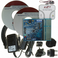
Evaluation Board, Power Supply, USB Cables, Adapter and Documentation
Processor To Be Evaluated
C8051F01x
Interface Type
USB
Silicon Manufacturer
Silicon Labs
Core Architecture
8051
Silicon Core Number
C8051F005
Silicon Family Name
C8051F00x
Lead Free Status / RoHS Status
Contains lead / RoHS non-compliant
For Use With/related Products
Silicon Laboratories C8051 F005/006/007
Lead Free Status / Rohs Status
Lead free / RoHS Compliant
Other names
336-1188
Available stocks
Company
Part Number
Manufacturer
Quantity
Price
Company:

Part Number:
C8051F005DK
Manufacturer:
SiliconL
Quantity:
1


15.3.
Each MCU has four byte-wide, bi-directional parallel ports that can be used general purpose I/O. Each port is
accessed through a corresponding special function register (SFR) that is both byte addressable and bit addressable.
When writing to a port, the value written to the SFR is latched to maintain the output data value at each pin. When
reading, the logic levels of the port’s input pins are returned regardless of the XBRn settings (i.e. even when the pin
is assigned to another signal by the Crossbar, the Port Register can always still read its corresponding Port I/O pin).
The exception to this is the execution of the read-modify-write instructions. The read-modify-write instructions
when operating on a port SFR are the following: ANL, ORL, XRL, JBC, CPL, INC, DEC, DJNZ and MOV, CLR
or SET, when the destination is an individual bit in a port SFR. For these instructions, the value of the port register
(not the pin) is read, modified, and written back to the SFR.
15.4.
P2 and P3 are not pinned out on the F001/06/11/16. P1, P2, and P3 are not pinned out on the F002/07/12/17. These
port registers (and corresponding interrupts, where applicable) are still available for software use in these reduced
pin count MCUs. Whether used or not in software, it is recommended not to let these port drivers go to high
impedance state. This is prevented after reset by having the weak pull-ups enabled as described in the XBR2
register. It is recommended that each output driver for ports not pinned out should be configured as push-pull using
the corresponding PRTnCF register. This will inhibit a high impedance state even if the weak pull-up is disabled.
109
C8051F000/1/2/5/6/7
C8051F010/1/2/5/6/7
Bits7-0: P0.[7:0]
Bits7-0: PRT0CF.[7:0]: Output Configuration Bits for P0.7-P0.0 (respectively)
P0.7
R/W
R/W
Bit7
Bit7
General Purpose Port I/O
Configuring Ports Which are not Pinned Out
(Write – Output appears on I/O pins per XBR0, XBR1, and XBR2 Registers)
0: Logic Low Output.
1: Logic High Output (high-impedance if corresponding PRT0CF.n bit = 0)
(Read – Regardless of XBR0, XBR1, and XBR2 Register settings).
0: P0.n pin is logic low.
1: P0.n pin is logic high.
0: Corresponding P0.n Output mode is Open-Drain.
1: Corresponding P0.n Output mode is Push-Pull.
(Note: When SDA, SCL, and RX appear on any of the P0 I/O, each are open-drain
P0.6
R/W
R/W
Bit6
Bit6
regardless of the value of PRT0CF).
Figure 15.7. PRT0CF: Port0 Configuration Register
P0.5
R/W
R/W
Bit5
Bit5
Figure 15.6. P0: Port0 Register
P0.4
R/W
R/W
Bit4
Bit4
Rev. 1.7
P0.3
R/W
R/W
Bit3
Bit3
P0.2
R/W
R/W
Bit2
Bit2
P0.1
R/W
R/W
Bit1
Bit1
(bit addressable)
P0.0
R/W
R/W
Bit0
Bit0
0x80
SFR Address:
SFR Address:
Reset Value
Reset Value
11111111
00000000
0xA4
Related parts for C8051F005DK
Image
Part Number
Description
Manufacturer
Datasheet
Request
R

Part Number:
Description:
SMD/C°/SINGLE-ENDED OUTPUT SILICON OSCILLATOR
Manufacturer:
Silicon Laboratories Inc
Part Number:
Description:
Manufacturer:
Silicon Laboratories Inc
Datasheet:
Part Number:
Description:
N/A N/A/SI4010 AES KEYFOB DEMO WITH LCD RX
Manufacturer:
Silicon Laboratories Inc
Datasheet:
Part Number:
Description:
N/A N/A/SI4010 SIMPLIFIED KEY FOB DEMO WITH LED RX
Manufacturer:
Silicon Laboratories Inc
Datasheet:
Part Number:
Description:
N/A/-40 TO 85 OC/EZLINK MODULE; F930/4432 HIGH BAND (REV E/B1)
Manufacturer:
Silicon Laboratories Inc
Part Number:
Description:
EZLink Module; F930/4432 Low Band (rev e/B1)
Manufacturer:
Silicon Laboratories Inc
Part Number:
Description:
I°/4460 10 DBM RADIO TEST CARD 434 MHZ
Manufacturer:
Silicon Laboratories Inc
Part Number:
Description:
I°/4461 14 DBM RADIO TEST CARD 868 MHZ
Manufacturer:
Silicon Laboratories Inc
Part Number:
Description:
I°/4463 20 DBM RFSWITCH RADIO TEST CARD 460 MHZ
Manufacturer:
Silicon Laboratories Inc
Part Number:
Description:
I°/4463 20 DBM RADIO TEST CARD 868 MHZ
Manufacturer:
Silicon Laboratories Inc
Part Number:
Description:
I°/4463 27 DBM RADIO TEST CARD 868 MHZ
Manufacturer:
Silicon Laboratories Inc
Part Number:
Description:
I°/4463 SKYWORKS 30 DBM RADIO TEST CARD 915 MHZ
Manufacturer:
Silicon Laboratories Inc
Part Number:
Description:
N/A N/A/-40 TO 85 OC/4463 RFMD 30 DBM RADIO TEST CARD 915 MHZ
Manufacturer:
Silicon Laboratories Inc
Part Number:
Description:
I°/4463 20 DBM RADIO TEST CARD 169 MHZ
Manufacturer:
Silicon Laboratories Inc