C8051F005DK Silicon Laboratories Inc, C8051F005DK Datasheet - Page 115
C8051F005DK
Manufacturer Part Number
C8051F005DK
Description
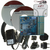
DEV KIT FOR F005/006/007
Manufacturer
Silicon Laboratories Inc
Type
MCUr
Datasheet
1.C8051F005-TB.pdf
(171 pages)
Specifications of C8051F005DK
Contents
Evaluation Board, Power Supply, USB Cables, Adapter and Documentation
Processor To Be Evaluated
C8051F01x
Interface Type
USB
Silicon Manufacturer
Silicon Labs
Core Architecture
8051
Silicon Core Number
C8051F005
Silicon Family Name
C8051F00x
Lead Free Status / RoHS Status
Contains lead / RoHS non-compliant
For Use With/related Products
Silicon Laboratories C8051 F005/006/007
Lead Free Status / Rohs Status
Lead free / RoHS Compliant
Other names
336-1188
Available stocks
Company
Part Number
Manufacturer
Quantity
Price
Company:

Part Number:
C8051F005DK
Manufacturer:
SiliconL
Quantity:
1


16.2.
A typical SMBus transaction consists of a START condition, followed by an address byte, one or more bytes of
data, and a STOP condition. The address byte and each of the data bytes are followed by an ACKNOWLEDGE bit
from the receiver. The address byte consists of a 7-bit address plus a direction bit. The direction bit (R/W)
occupies the least-significant bit position of the address. The direction bit is set to logic 1 to indicate a “READ”
operation and cleared to logic 0 to indicate a “WRITE” operation. A general call address (0x00 +R/W) is
recognized by all slave devices allowing a master to address multiple slave devices simultaneously.
All transactions are initiated by the master, with one or more addressed slave devices as the target.
generates the START condition and then transmits the address and direction bit. If the transaction is a WRITE
operation from the master to the slave, the master transmits the data a byte at a time waiting for an
ACKNOWLEDGE from the slave at the end of each byte. If it is a READ operation, the slave transmits the data
waiting for an ACKNOWLEDGE from the master at the end of each byte. At the end of the data transfer, the
master generates a STOP condition to terminate the transaction and free the bus. Figure 16.3 illustrates a typical
SMBus transaction.
The SMBus interface may be configured to operate as either a master or a slave. At any particular time, it will be
operating in one of the following four modes:
16.2.1. Master Transmitter Mode
Serial data is transmitted on SDA while the serial clock is output on SCL. The first byte transmitted contains the
address of the target slave device and the data direction bit. In this case the data direction bit (R/W) will be logic 0
to indicate a “WRITE” operation. The master then transmits one or more bytes of serial data. After each byte is
transmitted, an acknowledge bit is generated by the slave. To indicate the beginning and the end of the serial
transfer, the master device outputs START and STOP conditions.
16.2.2. Master Receiver Mode
Serial data is received on SDA while the serial clock is output on SCL. The first byte is transmitted by the master
and contains the address of the target slave and the data direction bit. In this case the data direction bit (R/W) will
be logic 1 to indicate a “READ” operation. Serial data is then received from the slave on SDA while the master
outputs the serial clock. The slave transmits one or more bytes of serial data. After each byte is received, an
acknowledge bit is transmitted by the master. The master outputs START and STOP conditions to indicate the
beginning and end of the serial transfer.
16.2.3. Slave Transmitter Mode
Serial data is transmitted on SDA while the serial clock is received on SCL. First, a byte is received that contains an
address and data direction bit. In this case the data direction bit (R/W) will be logic 1 to indicate a “READ”
operation. If the received address matches the slave’s assigned address (or a general call address is received) one or
more bytes of serial data are transmitted to the master. After each byte is received, an acknowledge bit is
transmitted by the master. The master outputs START and STOP conditions to indicate the beginning and end of
the serial transfer.
115
C8051F000/1/2/5/6/7
C8051F010/1/2/5/6/7
START
Operation
SLAVE ADDR R/W
Figure 16.3. SMBus Transaction
ACK
DATA
Rev. 1.7
Time
ACK
DATA
NACK
STOP
The master
Related parts for C8051F005DK
Image
Part Number
Description
Manufacturer
Datasheet
Request
R

Part Number:
Description:
SMD/C°/SINGLE-ENDED OUTPUT SILICON OSCILLATOR
Manufacturer:
Silicon Laboratories Inc
Part Number:
Description:
Manufacturer:
Silicon Laboratories Inc
Datasheet:
Part Number:
Description:
N/A N/A/SI4010 AES KEYFOB DEMO WITH LCD RX
Manufacturer:
Silicon Laboratories Inc
Datasheet:
Part Number:
Description:
N/A N/A/SI4010 SIMPLIFIED KEY FOB DEMO WITH LED RX
Manufacturer:
Silicon Laboratories Inc
Datasheet:
Part Number:
Description:
N/A/-40 TO 85 OC/EZLINK MODULE; F930/4432 HIGH BAND (REV E/B1)
Manufacturer:
Silicon Laboratories Inc
Part Number:
Description:
EZLink Module; F930/4432 Low Band (rev e/B1)
Manufacturer:
Silicon Laboratories Inc
Part Number:
Description:
I°/4460 10 DBM RADIO TEST CARD 434 MHZ
Manufacturer:
Silicon Laboratories Inc
Part Number:
Description:
I°/4461 14 DBM RADIO TEST CARD 868 MHZ
Manufacturer:
Silicon Laboratories Inc
Part Number:
Description:
I°/4463 20 DBM RFSWITCH RADIO TEST CARD 460 MHZ
Manufacturer:
Silicon Laboratories Inc
Part Number:
Description:
I°/4463 20 DBM RADIO TEST CARD 868 MHZ
Manufacturer:
Silicon Laboratories Inc
Part Number:
Description:
I°/4463 27 DBM RADIO TEST CARD 868 MHZ
Manufacturer:
Silicon Laboratories Inc
Part Number:
Description:
I°/4463 SKYWORKS 30 DBM RADIO TEST CARD 915 MHZ
Manufacturer:
Silicon Laboratories Inc
Part Number:
Description:
N/A N/A/-40 TO 85 OC/4463 RFMD 30 DBM RADIO TEST CARD 915 MHZ
Manufacturer:
Silicon Laboratories Inc
Part Number:
Description:
I°/4463 20 DBM RADIO TEST CARD 169 MHZ
Manufacturer:
Silicon Laboratories Inc