C8051F005DK Silicon Laboratories Inc, C8051F005DK Datasheet - Page 127
C8051F005DK
Manufacturer Part Number
C8051F005DK
Description
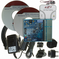
DEV KIT FOR F005/006/007
Manufacturer
Silicon Laboratories Inc
Type
MCUr
Datasheet
1.C8051F005-TB.pdf
(171 pages)
Specifications of C8051F005DK
Contents
Evaluation Board, Power Supply, USB Cables, Adapter and Documentation
Processor To Be Evaluated
C8051F01x
Interface Type
USB
Silicon Manufacturer
Silicon Labs
Core Architecture
8051
Silicon Core Number
C8051F005
Silicon Family Name
C8051F00x
Lead Free Status / RoHS Status
Contains lead / RoHS non-compliant
For Use With/related Products
Silicon Laboratories C8051 F005/006/007
Lead Free Status / Rohs Status
Lead free / RoHS Compliant
Other names
336-1188
Available stocks
Company
Part Number
Manufacturer
Quantity
Price
Company:

Part Number:
C8051F005DK
Manufacturer:
SiliconL
Quantity:
1


17.4.
The SPI is accessed and controlled through four special function registers in the system controller: SPI0CN Control
Register, SPI0DAT Data Register, SPI0CFG Configuration Register, and SPI0CKR Clock Rate Register. The four
special function registers related to the operation of the SPI Bus are described in the following section.
127
C8051F000/1/2/5/6/7
C8051F010/1/2/5/6/7
Bit7:
Bit6:
Bits5-3: BC2-BC0: SPI Bit Count.
Bits2-0: SPIFRS2-SPIFRS0: SPI Frame Size.
.
CKPHA
R/W
Bit7
SPI Special Function Registers
This bit controls the SPI clock phase.
0: Data sampled on first edge of SCK period.
1: Data sampled on second edge of SCK period.
This bit controls the SPI clock polarity.
0: SCK line low in idle state.
1: SCK line high in idle state.
Indicates which of the up to 8 bits of the SPI word have been transmitted.
These three bits determine the number of bits to shift in/out of the SPI shift register
during a data transfer in master mode. They are ignored in slave mode.
CKPHA: SPI Clock Phase.
CKPOL: SPI Clock Polarity.
CKPOL
0
0
0
0
1
1
1
1
0
0
0
0
1
1
1
1
R/W
Bit6
BC2-BC0
SPIFRS
Figure 17.5. SPI0CFG: SPI Configuration Register
0
0
1
1
0
0
1
1
0
0
1
1
0
0
1
1
BC2
Bit5
R
0
1
0
1
0
1
0
1
0
1
0
1
0
1
0
1
BC1
Bit4
Bits Shifted
Bit Transmitted
R
Bit 0 (LSB)
Bit 1
Bit 2
Bit 3
Bit 4
Bit 5
Bit 6
Bit 7 (MSB)
1
2
3
4
5
6
7
8
Rev. 1.7
BC0
Bit3
R
SPIFRS2
R/W
Bit2
SPIFRS1
R/W
Bit1
SPIFRS0
R/W
Bit0
SFR Address:
Reset Value
00000111
0x9A
Related parts for C8051F005DK
Image
Part Number
Description
Manufacturer
Datasheet
Request
R

Part Number:
Description:
SMD/C°/SINGLE-ENDED OUTPUT SILICON OSCILLATOR
Manufacturer:
Silicon Laboratories Inc
Part Number:
Description:
Manufacturer:
Silicon Laboratories Inc
Datasheet:
Part Number:
Description:
N/A N/A/SI4010 AES KEYFOB DEMO WITH LCD RX
Manufacturer:
Silicon Laboratories Inc
Datasheet:
Part Number:
Description:
N/A N/A/SI4010 SIMPLIFIED KEY FOB DEMO WITH LED RX
Manufacturer:
Silicon Laboratories Inc
Datasheet:
Part Number:
Description:
N/A/-40 TO 85 OC/EZLINK MODULE; F930/4432 HIGH BAND (REV E/B1)
Manufacturer:
Silicon Laboratories Inc
Part Number:
Description:
EZLink Module; F930/4432 Low Band (rev e/B1)
Manufacturer:
Silicon Laboratories Inc
Part Number:
Description:
I°/4460 10 DBM RADIO TEST CARD 434 MHZ
Manufacturer:
Silicon Laboratories Inc
Part Number:
Description:
I°/4461 14 DBM RADIO TEST CARD 868 MHZ
Manufacturer:
Silicon Laboratories Inc
Part Number:
Description:
I°/4463 20 DBM RFSWITCH RADIO TEST CARD 460 MHZ
Manufacturer:
Silicon Laboratories Inc
Part Number:
Description:
I°/4463 20 DBM RADIO TEST CARD 868 MHZ
Manufacturer:
Silicon Laboratories Inc
Part Number:
Description:
I°/4463 27 DBM RADIO TEST CARD 868 MHZ
Manufacturer:
Silicon Laboratories Inc
Part Number:
Description:
I°/4463 SKYWORKS 30 DBM RADIO TEST CARD 915 MHZ
Manufacturer:
Silicon Laboratories Inc
Part Number:
Description:
N/A N/A/-40 TO 85 OC/4463 RFMD 30 DBM RADIO TEST CARD 915 MHZ
Manufacturer:
Silicon Laboratories Inc
Part Number:
Description:
I°/4463 20 DBM RADIO TEST CARD 169 MHZ
Manufacturer:
Silicon Laboratories Inc