C8051F005DK Silicon Laboratories Inc, C8051F005DK Datasheet - Page 128
C8051F005DK
Manufacturer Part Number
C8051F005DK
Description
DEV KIT FOR F005/006/007
Manufacturer
Silicon Laboratories Inc
Type
MCUr
Datasheet
1.C8051F005-TB.pdf
(171 pages)
Specifications of C8051F005DK
Contents
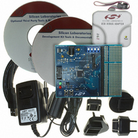
Evaluation Board, Power Supply, USB Cables, Adapter and Documentation
Processor To Be Evaluated
C8051F01x
Interface Type
USB
Silicon Manufacturer
Silicon Labs
Core Architecture
8051
Silicon Core Number
C8051F005
Silicon Family Name
C8051F00x
Lead Free Status / RoHS Status
Contains lead / RoHS non-compliant
For Use With/related Products
Silicon Laboratories C8051 F005/006/007
Lead Free Status / Rohs Status
Lead free / RoHS Compliant
Other names
336-1188
Available stocks
Company
Part Number
Manufacturer
Quantity
Price
Company:

Part Number:
C8051F005DK
Manufacturer:
SiliconL
Quantity:
1


Bit7:
Bit6:
Bit5:
Bit4:
Bit3:
Bit2:
Bit1:
Bit0:
SPIF
R/W
Bit7
This bit is set to logic 1 by hardware at the end of a data transfer. If interrupts are enabled,
setting this bit causes the CPU to vector to the SPI0 interrupt service routine. This bit is
not automatically cleared by hardware. It must be cleared by software.
WCOL: Write Collision Flag.
This bit is set to logic 1 by hardware (and generates a SPI interrupt) to indicate a write to
the SPI data register was attempted while a data transfer was in progress. It is cleared by
software.
This bit is set to logic 1 by hardware (and generates a SPI interrupt) when a master mode
collision is detected (NSS is low and MSTEN = 1). This bit is not automatically cleared by
hardware. It must be cleared by software.
This bit is set to logic 1 by hardware (and generates a SPI interrupt) when the receive
buffer still holds unread data from a previous transfer and the last bit of the current transfer
is shifted into the SPI shift register. This bit is not automatically cleared by hardware. It
must be cleared by software.
This bit is set to logic 1 by hardware while a master mode transfer is in progress. It is
cleared by hardware at the end of the transfer.
This bit is set to logic 1 whenever the NSS pin is low indicating it is enabled as a slave. It
is cleared to logic 0 when NSS is high (slave disabled).
0: Disable master mode. Operate in slave mode.
1: Enable master mode. Operate as a master.
This bit enables/disables the SPI.
0: SPI disabled.
1: SPI enabled.
SPIF: SPI Interrupt Flag.
MODF: Mode Fault Flag.
RXOVRN: Receive Overrun Flag.
TXBSY: Transmit Busy Flag.
SLVSEL: Slave Selected Flag.
MSTEN: Master Mode Enable.
SPIEN: SPI Enable.
WCOL
R/W
Bit6
Figure 17.6. SPI0CN: SPI Control Register
MODF
R/W
Bit5
RXOVRN
R/W
Bit4
Rev. 1.7
TXBSY
Bit3
R
SLVSEL
Bit2
R
C8051F000/1/2/5/6/7
C8051F010/1/2/5/6/7
MSTEN
R/W
Bit1
(bit addressable)
SPIEN
R/W
Bit0
SFR Address:
Reset Value
00000000
0xF8
128
Related parts for C8051F005DK
Image
Part Number
Description
Manufacturer
Datasheet
Request
R

Part Number:
Description:
SMD/C°/SINGLE-ENDED OUTPUT SILICON OSCILLATOR
Manufacturer:
Silicon Laboratories Inc
Part Number:
Description:
Manufacturer:
Silicon Laboratories Inc
Datasheet:
Part Number:
Description:
N/A N/A/SI4010 AES KEYFOB DEMO WITH LCD RX
Manufacturer:
Silicon Laboratories Inc
Datasheet:
Part Number:
Description:
N/A N/A/SI4010 SIMPLIFIED KEY FOB DEMO WITH LED RX
Manufacturer:
Silicon Laboratories Inc
Datasheet:
Part Number:
Description:
N/A/-40 TO 85 OC/EZLINK MODULE; F930/4432 HIGH BAND (REV E/B1)
Manufacturer:
Silicon Laboratories Inc
Part Number:
Description:
EZLink Module; F930/4432 Low Band (rev e/B1)
Manufacturer:
Silicon Laboratories Inc
Part Number:
Description:
I°/4460 10 DBM RADIO TEST CARD 434 MHZ
Manufacturer:
Silicon Laboratories Inc
Part Number:
Description:
I°/4461 14 DBM RADIO TEST CARD 868 MHZ
Manufacturer:
Silicon Laboratories Inc
Part Number:
Description:
I°/4463 20 DBM RFSWITCH RADIO TEST CARD 460 MHZ
Manufacturer:
Silicon Laboratories Inc
Part Number:
Description:
I°/4463 20 DBM RADIO TEST CARD 868 MHZ
Manufacturer:
Silicon Laboratories Inc
Part Number:
Description:
I°/4463 27 DBM RADIO TEST CARD 868 MHZ
Manufacturer:
Silicon Laboratories Inc
Part Number:
Description:
I°/4463 SKYWORKS 30 DBM RADIO TEST CARD 915 MHZ
Manufacturer:
Silicon Laboratories Inc
Part Number:
Description:
N/A N/A/-40 TO 85 OC/4463 RFMD 30 DBM RADIO TEST CARD 915 MHZ
Manufacturer:
Silicon Laboratories Inc
Part Number:
Description:
I°/4463 20 DBM RADIO TEST CARD 169 MHZ
Manufacturer:
Silicon Laboratories Inc