C8051F005DK Silicon Laboratories Inc, C8051F005DK Datasheet - Page 168
C8051F005DK
Manufacturer Part Number
C8051F005DK
Description
DEV KIT FOR F005/006/007
Manufacturer
Silicon Laboratories Inc
Type
MCUr
Datasheet
1.C8051F005-TB.pdf
(171 pages)
Specifications of C8051F005DK
Contents
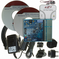
Evaluation Board, Power Supply, USB Cables, Adapter and Documentation
Processor To Be Evaluated
C8051F01x
Interface Type
USB
Silicon Manufacturer
Silicon Labs
Core Architecture
8051
Silicon Core Number
C8051F005
Silicon Family Name
C8051F00x
Lead Free Status / RoHS Status
Contains lead / RoHS non-compliant
For Use With/related Products
Silicon Laboratories C8051 F005/006/007
Lead Free Status / Rohs Status
Lead free / RoHS Compliant
Other names
336-1188
Available stocks
Company
Part Number
Manufacturer
Quantity
Price
Company:

Part Number:
C8051F005DK
Manufacturer:
SiliconL
Quantity:
1


Bit15
WRMD3
This register determines how the Flash interface logic will respond to reads and writes to the
FLASHDAT Register.
Bits7-4: WRMD3-0: Write Mode Select Bits.
Bits3-0: RDMD3-0: Read Mode Select Bits.
This register holds the address for all JTAG Flash read, write, and erase operations. This register
autoincrements after each read or write, regardless of whether the operation succeeded or failed.
Bits15-0: Flash Operation 16-bit Address.
Bit7
The Write Mode Select Bits control how the interface logic responds to writes to the
FLASHDAT Register per the following values:
0000: A FLASHDAT write replaces the data in the FLASHDAT register, but is otherwise
0001: A FLASHDAT write initiates a write of FLASHDAT into the memory location
0010: A FLASHDAT write initiates an erasure (sets all bytes to 0xFF) of the Flash page
(All other values for WRMD3-0 are reserved.)
The Read Mode Select Bits control how the interface logic responds to reads to the
FLASHDAT Register per the following values:
0000: A FLASHDAT read provides the data in the FASHDAT register, but is otherwise
0001: A FLASHDAT read initiates a read of the byte addressed by the FLASHADR register
0010: A FLASHDAT read initiates a read of the byte addressed by FLASHADR only if no
(All other values for RDMD3-0 are reserved.)
WRMD2
Bit6
ignored.
addressed by the FLASHADR register. FLASHADR is incremented by one when
complete.
containing the address in FLASHADR. FLASHDAT must be 0xA5 for the erase to
occur. FLASHADR is not affected. If FLASHADR = 0x7DFE – 0x7DFF, the entire
user space will be erased (i.e. entire Flash memory except for Reserved area 0x7E00 –
0x7FFF).
ignored.
if no operation is currently active. This mode is used for block reads.
operation is active and any data from a previous read has already been read from
FLASHDAT. This mode allows single bytes to be read (or the last byte of a block)
without initiating an extra read.
Figure 21.4. FLASHADR: JTAG Flash Address Register
Figure 21.3. FLASHCON: JTAG Flash Control Register
WRMD1
Bit5
WRMD0
Bit4
Rev. 1.7
RDMD3
Bit3
RDMD2
Bit2
C8051F000/1/2/5/6/7
C8051F010/1/2/5/6/7
RDMD1
Bit1
RDMD0
Bit0
Bit0
Reset Value
Reset Value
00000000
0x0000
168
Related parts for C8051F005DK
Image
Part Number
Description
Manufacturer
Datasheet
Request
R

Part Number:
Description:
SMD/C°/SINGLE-ENDED OUTPUT SILICON OSCILLATOR
Manufacturer:
Silicon Laboratories Inc
Part Number:
Description:
Manufacturer:
Silicon Laboratories Inc
Datasheet:
Part Number:
Description:
N/A N/A/SI4010 AES KEYFOB DEMO WITH LCD RX
Manufacturer:
Silicon Laboratories Inc
Datasheet:
Part Number:
Description:
N/A N/A/SI4010 SIMPLIFIED KEY FOB DEMO WITH LED RX
Manufacturer:
Silicon Laboratories Inc
Datasheet:
Part Number:
Description:
N/A/-40 TO 85 OC/EZLINK MODULE; F930/4432 HIGH BAND (REV E/B1)
Manufacturer:
Silicon Laboratories Inc
Part Number:
Description:
EZLink Module; F930/4432 Low Band (rev e/B1)
Manufacturer:
Silicon Laboratories Inc
Part Number:
Description:
I°/4460 10 DBM RADIO TEST CARD 434 MHZ
Manufacturer:
Silicon Laboratories Inc
Part Number:
Description:
I°/4461 14 DBM RADIO TEST CARD 868 MHZ
Manufacturer:
Silicon Laboratories Inc
Part Number:
Description:
I°/4463 20 DBM RFSWITCH RADIO TEST CARD 460 MHZ
Manufacturer:
Silicon Laboratories Inc
Part Number:
Description:
I°/4463 20 DBM RADIO TEST CARD 868 MHZ
Manufacturer:
Silicon Laboratories Inc
Part Number:
Description:
I°/4463 27 DBM RADIO TEST CARD 868 MHZ
Manufacturer:
Silicon Laboratories Inc
Part Number:
Description:
I°/4463 SKYWORKS 30 DBM RADIO TEST CARD 915 MHZ
Manufacturer:
Silicon Laboratories Inc
Part Number:
Description:
N/A N/A/-40 TO 85 OC/4463 RFMD 30 DBM RADIO TEST CARD 915 MHZ
Manufacturer:
Silicon Laboratories Inc
Part Number:
Description:
I°/4463 20 DBM RADIO TEST CARD 169 MHZ
Manufacturer:
Silicon Laboratories Inc