C8051F005DK Silicon Laboratories Inc, C8051F005DK Datasheet - Page 51
C8051F005DK
Manufacturer Part Number
C8051F005DK
Description
DEV KIT FOR F005/006/007
Manufacturer
Silicon Laboratories Inc
Type
MCUr
Datasheet
1.C8051F005-TB.pdf
(171 pages)
Specifications of C8051F005DK
Contents
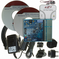
Evaluation Board, Power Supply, USB Cables, Adapter and Documentation
Processor To Be Evaluated
C8051F01x
Interface Type
USB
Silicon Manufacturer
Silicon Labs
Core Architecture
8051
Silicon Core Number
C8051F005
Silicon Family Name
C8051F00x
Lead Free Status / RoHS Status
Contains lead / RoHS non-compliant
For Use With/related Products
Silicon Laboratories C8051 F005/006/007
Lead Free Status / Rohs Status
Lead free / RoHS Compliant
Other names
336-1188
Available stocks
Company
Part Number
Manufacturer
Quantity
Price
Company:

Part Number:
C8051F005DK
Manufacturer:
SiliconL
Quantity:
1


7. DACs, 12 BIT VOLTAGE MODE
The C8051F000 MCU family has two 12-bit voltage-mode Digital to Analog Converters. Each DAC has an output
swing of 0V to VREF-1LSB for a corresponding input code range of 0x000 to 0xFFF. Using DAC0 as an example,
the 12-bit data word is written to the low byte (DAC0L) and high byte (DAC0H) data registers. Data is latched into
DAC0 after a write to the corresponding DAC0H register, so the write sequence should be DAC0L followed by
DAC0H if the full 12-bit resolution is required. The DAC can be used in 8-bit mode by initializing DAC0L to the
desired value (typically 0x00), and writing data to only DAC0H with the data shifted to the left. DAC0 Control
Register (DAC0CN) provides a means to enable/disable DAC0 and to modify its input data formatting.
The DAC0 enable/disable function is controlled by the DAC0EN bit (DAC0CN.7). Writing a 1 to DAC0EN
enables DAC0 while writing a 0 to DAC0EN disables DAC0. While disabled, the output of DAC0 is maintained in
a high-impedance state, and the DAC0 supply current falls to 1A or less. Also, the Bias Enable bit (BIASE) in the
REF0CN register (see Figure 9.2) must be set to 1 in order to supply bias to DAC0. The voltage reference for
DAC0 must also be set properly (see Section 9).
In some instances, input data should be shifted prior to a DAC0 write operation to properly justify data within the
DAC input registers. This action would typically require one or more load and shift operations, adding software
overhead and slowing DAC throughput. To alleviate this problem, the data-formatting feature provides a means for
the user to program the orientation of the DAC0 data word within data registers DAC0H and DAC0L. The three
DAC0DF bits (DAC0CN.[2:0]) allow the user to specify one of five data word orientations as shown in the
DAC0CN register definition.
DAC1 is functionally the same as DAC0 described above. The electrical specifications for both DAC0 and DAC1
are given in Table 7.1.
51
C8051F000/1/2/5/6/7
C8051F010/1/2/5/6/7
DAC0DF2
DAC0DF1
DAC0DF0
DAC1DF2
DAC1DF1
DAC1DF0
DAC0EN
DAC1EN
Figure 7.1. DAC Functional Block Diagram
8
8
8
8
12
12
Rev. 1.7
REF
REF
DAC0
DAC1
+
-
+
-
AGND
AGND
AV+
AV+
DAC0
DAC1
Related parts for C8051F005DK
Image
Part Number
Description
Manufacturer
Datasheet
Request
R

Part Number:
Description:
SMD/C°/SINGLE-ENDED OUTPUT SILICON OSCILLATOR
Manufacturer:
Silicon Laboratories Inc
Part Number:
Description:
Manufacturer:
Silicon Laboratories Inc
Datasheet:
Part Number:
Description:
N/A N/A/SI4010 AES KEYFOB DEMO WITH LCD RX
Manufacturer:
Silicon Laboratories Inc
Datasheet:
Part Number:
Description:
N/A N/A/SI4010 SIMPLIFIED KEY FOB DEMO WITH LED RX
Manufacturer:
Silicon Laboratories Inc
Datasheet:
Part Number:
Description:
N/A/-40 TO 85 OC/EZLINK MODULE; F930/4432 HIGH BAND (REV E/B1)
Manufacturer:
Silicon Laboratories Inc
Part Number:
Description:
EZLink Module; F930/4432 Low Band (rev e/B1)
Manufacturer:
Silicon Laboratories Inc
Part Number:
Description:
I°/4460 10 DBM RADIO TEST CARD 434 MHZ
Manufacturer:
Silicon Laboratories Inc
Part Number:
Description:
I°/4461 14 DBM RADIO TEST CARD 868 MHZ
Manufacturer:
Silicon Laboratories Inc
Part Number:
Description:
I°/4463 20 DBM RFSWITCH RADIO TEST CARD 460 MHZ
Manufacturer:
Silicon Laboratories Inc
Part Number:
Description:
I°/4463 20 DBM RADIO TEST CARD 868 MHZ
Manufacturer:
Silicon Laboratories Inc
Part Number:
Description:
I°/4463 27 DBM RADIO TEST CARD 868 MHZ
Manufacturer:
Silicon Laboratories Inc
Part Number:
Description:
I°/4463 SKYWORKS 30 DBM RADIO TEST CARD 915 MHZ
Manufacturer:
Silicon Laboratories Inc
Part Number:
Description:
N/A N/A/-40 TO 85 OC/4463 RFMD 30 DBM RADIO TEST CARD 915 MHZ
Manufacturer:
Silicon Laboratories Inc
Part Number:
Description:
I°/4463 20 DBM RADIO TEST CARD 169 MHZ
Manufacturer:
Silicon Laboratories Inc