C8051F005DK Silicon Laboratories Inc, C8051F005DK Datasheet - Page 68
C8051F005DK
Manufacturer Part Number
C8051F005DK
Description
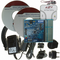
DEV KIT FOR F005/006/007
Manufacturer
Silicon Laboratories Inc
Type
MCUr
Datasheet
1.C8051F005-TB.pdf
(171 pages)
Specifications of C8051F005DK
Contents
Evaluation Board, Power Supply, USB Cables, Adapter and Documentation
Processor To Be Evaluated
C8051F01x
Interface Type
USB
Silicon Manufacturer
Silicon Labs
Core Architecture
8051
Silicon Core Number
C8051F005
Silicon Family Name
C8051F00x
Lead Free Status / RoHS Status
Contains lead / RoHS non-compliant
For Use With/related Products
Silicon Laboratories C8051 F005/006/007
Lead Free Status / Rohs Status
Lead free / RoHS Compliant
Other names
336-1188
Available stocks
Company
Part Number
Manufacturer
Quantity
Price
Company:

Part Number:
C8051F005DK
Manufacturer:
SiliconL
Quantity:
1


10.2.
The memory organization of the CIP-51 System Controller is similar to that of a standard 8051. There are two
separate memory spaces: program memory and data memory. Program and data memory share the same address
space but are accessed via different instruction types. There are 256 bytes of internal data memory and 64K bytes of
internal program memory address space implemented within the CIP-51. The CIP-51 memory organization is
shown in Figure 10.2.
10.2.1. Program Memory
The CIP-51 has a 64K-byte program memory space. The MCU implements 32896 bytes of this program memory
space as in-system, reprogrammable Flash memory, organized in a contiguous block from addresses 0x0000 to
0x807F. Note: 512 bytes (0x7E00 – 0x7FFF) of this memory are reserved for factory use and are not available for
user program storage.
Program memory is normally assumed to be read-only. However, the CIP-51 can write to program memory by
setting the Program Store Write Enable bit (PSCTL.0) and using the MOVX instruction. This feature provides a
mechanism for the CIP-51 to update program code and use the program memory space for non-volatile data storage.
Refer to Section 11 (Flash Memory) for further details.
10.2.2. Data Memory
The CIP-51 implements 256 bytes of internal RAM mapped into the data memory space from 0x00 through 0xFF.
The lower 128 bytes of data memory are used for general purpose registers and scratch pad memory. Either direct
or indirect addressing may be used to access the lower 128 bytes of data memory. Locations 0x00 through 0x1F are
addressable as four banks of general purpose registers, each bank consisting of eight byte-wide registers. The next
16 bytes, locations 0x20 through 0x2F, may be addressed as bytes or as 128 bit locations accessible with the direct-
bit addressing mode.
The upper 128 bytes of data memory are accessible only by indirect addressing. This region occupies the same
address space as the Special Function Registers (SFR) but is physically separate from the SFR space. The
addressing mode used by an instruction when accessing locations above 0x7F determines whether the CPU accesses
the upper 128 bytes of data memory space or the SFRs. Instructions that use direct addressing will access the SFR
space. Instructions using indirect addressing above 0x7F will access the upper 128 bytes of data memory. Figure
10.2 illustrates the data memory organization of the CIP-51.
The C8051F005/06/07/15/16/17 also have 2048 bytes of RAM in the external data memory space of the CIP-51,
accessible using the MOVX instruction. Refer to Section 12 (External RAM) for details.
10.2.3. General Purpose Registers
The lower 32 bytes of data memory, locations 0x00 through 0x1F, may be addressed as four banks of general-
purpose registers. Each bank consists of eight byte-wide registers designated R0 through R7. Only one of these
banks may be enabled at a time. Two bits in the program status word, RS0 (PSW.3) and RS1 (PSW.4), select the
active register bank (see description of the PSW in Figure 10.6). This allows fast context switching when entering
subroutines and interrupt service routines. Indirect addressing modes use registers R0 and R1 as index registers.
10.2.4. Bit Addressable Locations
In addition to direct access to data memory organized as bytes, the sixteen data memory locations at 0x20 through
0x2F are also accessible as 128 individually addressable bits. Each bit has a bit address from 0x00 to 0x7F. Bit 0
of the byte at 0x20 has bit address 0x00 while bit 7 of the byte at 0x20 has bit address 0x07. Bit 7 of the byte at
0x2F has bit address 0x7F. A bit access is distinguished from a full byte access by the type of instruction used (bit
source or destination operands as opposed to a byte source or destination).
The MCS-51™ assembly language allows an alternate notation for bit addressing of the form XX.B where XX is the
byte address and B is the bit position within the byte. For example, the instruction:
moves the Boolean value at 0x13 (bit 3 of the byte at location 0x22) into the user Carry flag.
MOV
MEMORY ORGANIZATION
C, 22h.3
Rev. 1.7
C8051F000/1/2/5/6/7
C8051F010/1/2/5/6/7
68
Related parts for C8051F005DK
Image
Part Number
Description
Manufacturer
Datasheet
Request
R

Part Number:
Description:
SMD/C°/SINGLE-ENDED OUTPUT SILICON OSCILLATOR
Manufacturer:
Silicon Laboratories Inc
Part Number:
Description:
Manufacturer:
Silicon Laboratories Inc
Datasheet:
Part Number:
Description:
N/A N/A/SI4010 AES KEYFOB DEMO WITH LCD RX
Manufacturer:
Silicon Laboratories Inc
Datasheet:
Part Number:
Description:
N/A N/A/SI4010 SIMPLIFIED KEY FOB DEMO WITH LED RX
Manufacturer:
Silicon Laboratories Inc
Datasheet:
Part Number:
Description:
N/A/-40 TO 85 OC/EZLINK MODULE; F930/4432 HIGH BAND (REV E/B1)
Manufacturer:
Silicon Laboratories Inc
Part Number:
Description:
EZLink Module; F930/4432 Low Band (rev e/B1)
Manufacturer:
Silicon Laboratories Inc
Part Number:
Description:
I°/4460 10 DBM RADIO TEST CARD 434 MHZ
Manufacturer:
Silicon Laboratories Inc
Part Number:
Description:
I°/4461 14 DBM RADIO TEST CARD 868 MHZ
Manufacturer:
Silicon Laboratories Inc
Part Number:
Description:
I°/4463 20 DBM RFSWITCH RADIO TEST CARD 460 MHZ
Manufacturer:
Silicon Laboratories Inc
Part Number:
Description:
I°/4463 20 DBM RADIO TEST CARD 868 MHZ
Manufacturer:
Silicon Laboratories Inc
Part Number:
Description:
I°/4463 27 DBM RADIO TEST CARD 868 MHZ
Manufacturer:
Silicon Laboratories Inc
Part Number:
Description:
I°/4463 SKYWORKS 30 DBM RADIO TEST CARD 915 MHZ
Manufacturer:
Silicon Laboratories Inc
Part Number:
Description:
N/A N/A/-40 TO 85 OC/4463 RFMD 30 DBM RADIO TEST CARD 915 MHZ
Manufacturer:
Silicon Laboratories Inc
Part Number:
Description:
I°/4463 20 DBM RADIO TEST CARD 169 MHZ
Manufacturer:
Silicon Laboratories Inc