C8051F020DK Silicon Laboratories Inc, C8051F020DK Datasheet - Page 139
C8051F020DK
Manufacturer Part Number
C8051F020DK
Description
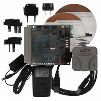
DEV KIT FOR F020/F021/F022/F023
Manufacturer
Silicon Laboratories Inc
Type
MCUr
Datasheet
1.C8051F020DK.pdf
(272 pages)
Specifications of C8051F020DK
Contents
Evaluation Board, Power Supply, USB Cables, Adapter and Documentation
Processor To Be Evaluated
C8051F02x
Interface Type
USB
Silicon Manufacturer
Silicon Labs
Core Architecture
8051
Silicon Core Number
C8051F020
Silicon Family Name
C8051F02x
Lead Free Status / RoHS Status
Contains lead / RoHS non-compliant
For Use With/related Products
Silicon Laboratories C8051 F020/021/022/023
Lead Free Status / Rohs Status
Lead free / RoHS Compliant
Other names
336-1200
Available stocks
Company
Part Number
Manufacturer
Quantity
Price
Company:

Part Number:
C8051F020DK
Manufacturer:
SiliconL
Quantity:
10


15.
The C8051F020/1/2/3 family includes 64k + 128 bytes of on-chip, reprogrammable FLASH memory for program
code and non-volatile data storage. The FLASH memory can be programmed in-system, a single byte at a time,
through the JTAG interface or by software. Once cleared to logic 0, a FLASH bit must be erased to set it back to
logic 1. The bytes would typically be erased (set to 0xFF) before being reprogrammed. FLASH write and erase oper-
ations are automatically timed by hardware for proper execution; data polling to determine the end of the write/erase
operation is not required. Refer to Table 15.1 for the electrical characteristics of the FLASH memory.
15.1. Programming The FLASH Memory
The simplest means of programming the FLASH memory is through the JTAG interface using programming tools
provided by Silicon Labs or a third party vendor. This is the only means for programming a non-initialized device.
For details on the JTAG commands to program FLASH memory, see
mands” on page
The FLASH memory can be programmed by software using a MOVX write instruction, with the address and data
byte to be programmed provided as normal operands. Before writing to FLASH memory using a MOVX write,
FLASH write operations must be enabled by setting the PSWE Program Store Write Enable bit (PSCTL.0) to logic 1.
This directs the MOVX writes to FLASH memory instead of XRAM. The PSWE bit remains set until cleared by soft-
ware. To avoid errant FLASH writes, it is recommended that interrupts be disabled while the PSWE bit is logic 1.
FLASH memory is read using the MOVC read instruction. MOVX reads are always directed to XRAM, regardless of
the state of PSWE.
To ensure the integrity of FLASH contents, it is strongly recommended that the on-chip VDD monitor be
enabled by tying the MONEN pin to VDD in any system which includes code that writes to or erases FLASH
memory from software.
A write to FLASH memory can clear bits but cannot set them; only an erase operation can set bits in FLASH. A byte
location to be programmed must be erased before a new value can be written. The 64k byte FLASH memory is
organized in 512-byte pages. The erase operation applies to an entire page (setting all bytes in the page to 0xFF). The
following steps illustrate the algorithm for programming FLASH by user software.
FLASH MEMORY
Step 1. Disable interrupts.
Step 2. Set FLWE (FLSCL.0) to enable FLASH writes/erases via user software.
Step 3. Set PSEE (PSCTL.1) to enable FLASH erases.
Step 4. Set PSWE (PSCTL.0) to redirect MOVX commands to write to FLASH.
Step 5. Use the MOVX command to write a data byte to any location within the 512-byte page to be erased.
Step 6. Clear PSEE to disable FLASH erases
Step 7. Use the MOVX command to write a data byte to the desired byte location within the erased 512-byte
Step 8. Clear the PSWE bit to redirect MOVX commands to the XRAM data space.
Step 9. Re-enable interrupts.
page. Repeat this step until all desired bytes are written (within the target page).
268.
Rev. 1.4
Section “24.2. Flash Programming Com-
C8051F020/1/2/3
139
Related parts for C8051F020DK
Image
Part Number
Description
Manufacturer
Datasheet
Request
R

Part Number:
Description:
SMD/C°/SINGLE-ENDED OUTPUT SILICON OSCILLATOR
Manufacturer:
Silicon Laboratories Inc
Part Number:
Description:
Manufacturer:
Silicon Laboratories Inc
Datasheet:
Part Number:
Description:
N/A N/A/SI4010 AES KEYFOB DEMO WITH LCD RX
Manufacturer:
Silicon Laboratories Inc
Datasheet:
Part Number:
Description:
N/A N/A/SI4010 SIMPLIFIED KEY FOB DEMO WITH LED RX
Manufacturer:
Silicon Laboratories Inc
Datasheet:
Part Number:
Description:
N/A/-40 TO 85 OC/EZLINK MODULE; F930/4432 HIGH BAND (REV E/B1)
Manufacturer:
Silicon Laboratories Inc
Part Number:
Description:
EZLink Module; F930/4432 Low Band (rev e/B1)
Manufacturer:
Silicon Laboratories Inc
Part Number:
Description:
I°/4460 10 DBM RADIO TEST CARD 434 MHZ
Manufacturer:
Silicon Laboratories Inc
Part Number:
Description:
I°/4461 14 DBM RADIO TEST CARD 868 MHZ
Manufacturer:
Silicon Laboratories Inc
Part Number:
Description:
I°/4463 20 DBM RFSWITCH RADIO TEST CARD 460 MHZ
Manufacturer:
Silicon Laboratories Inc
Part Number:
Description:
I°/4463 20 DBM RADIO TEST CARD 868 MHZ
Manufacturer:
Silicon Laboratories Inc
Part Number:
Description:
I°/4463 27 DBM RADIO TEST CARD 868 MHZ
Manufacturer:
Silicon Laboratories Inc
Part Number:
Description:
I°/4463 SKYWORKS 30 DBM RADIO TEST CARD 915 MHZ
Manufacturer:
Silicon Laboratories Inc
Part Number:
Description:
N/A N/A/-40 TO 85 OC/4463 RFMD 30 DBM RADIO TEST CARD 915 MHZ
Manufacturer:
Silicon Laboratories Inc
Part Number:
Description:
I°/4463 20 DBM RADIO TEST CARD 169 MHZ
Manufacturer:
Silicon Laboratories Inc