C8051F020DK Silicon Laboratories Inc, C8051F020DK Datasheet - Page 177
C8051F020DK
Manufacturer Part Number
C8051F020DK
Description
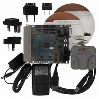
DEV KIT FOR F020/F021/F022/F023
Manufacturer
Silicon Laboratories Inc
Type
MCUr
Datasheet
1.C8051F020DK.pdf
(272 pages)
Specifications of C8051F020DK
Contents
Evaluation Board, Power Supply, USB Cables, Adapter and Documentation
Processor To Be Evaluated
C8051F02x
Interface Type
USB
Silicon Manufacturer
Silicon Labs
Core Architecture
8051
Silicon Core Number
C8051F020
Silicon Family Name
C8051F02x
Lead Free Status / RoHS Status
Contains lead / RoHS non-compliant
For Use With/related Products
Silicon Laboratories C8051 F020/021/022/023
Lead Free Status / Rohs Status
Lead free / RoHS Compliant
Other names
336-1200
Available stocks
Company
Part Number
Manufacturer
Quantity
Price
Company:

Part Number:
C8051F020DK
Manufacturer:
SiliconL
Quantity:
10


17.2. Ports 4 through 7 (C8051F020/2 only)
All Port pins on Ports 4 through 7 can be accessed as General-Purpose I/O (GPIO) pins by reading and writing the
associated Port Data registers (See Figure 17.21, Figure 17.22, Figure 17.23, and Figure 17.24), a set of SFRs which
are byte-addressable.
A Read of a Port Data register (or Port bit) will always return the logic state present at the pin itself, regardless of
whether the Crossbar has allocated the pin for peripheral use or not. An exception to this occurs during the execution
of a read-modify-write instruction (ANL, ORL, XRL, CPL, INC, DEC, DJNZ, JBC, CLR, SET, and the bitwise MOV
operation). During the read cycle of the read-modify-write instruction, it is the contents of the Port Data register, not
the state of the Port pins themselves, which is read.
17.2.1. Configuring Ports which are not Pinned Out
Although P4, P5, P6, and P7 are not brought out to pins on the C8051F021/3 devices, the Port Data registers are still
present and can be used by software. Because the digital input paths also remain active, it is recommended that these
pins not be left in a ‘floating’ state in order to avoid unnecessary power dissipation arising from the inputs floating to
non-valid logic levels. This condition can be prevented by any of the following:
17.2.2. Configuring the Output Modes of the Port Pins
The output mode of each port pin can be configured to be either Open-Drain or Push-Pull. In the Push-Pull configura-
tion, a logic 0 in the associated bit in the Port Data register will cause the Port pin to be driven to GND, and a logic 1
will cause the Port pin to be driven to VDD. In the Open-Drain configuration, a logic 0 in the associated bit in the
Bit7:
Bit6:
Bits5-4:
Bit3:
Bit2:
Bits1-0:
R/W
IE7
Bit7
1.
2.
3.
IE7: External Interrupt 7 Pending Flag
0: No falling edge has been detected on P3.7 since this bit was last cleared.
1: This flag is set by hardware when a falling edge on P3.7 is detected.
IE6: External Interrupt 6 Pending Flag
0: No falling edge has been detected on P3.6 since this bit was last cleared.
1: This flag is set by hardware when a falling edge on P3.6 is detected.
UNUSED. Read = 00b, Write = don’t care.
IE7CF: External Interrupt 7 Edge Configuration
0: External Interrupt 7 triggered by a falling edge on the IE7 input.
1: External Interrupt 7 triggered by a rising edge on the IE7 input.
IE6CF: External Interrupt 6 Edge Configuration
0: External Interrupt 6 triggered by a falling edge on the IE6 input.
1: External Interrupt 6 triggered by a rising edge on the IE6 input.
UNUSED. Read = 00b, Write = don’t care.
Leave the weak pull-up devices enabled by setting WEAKPUD (XBR2.7) to a logic 0.
Configure the output modes of P4, P5, P6, and P7 to “Push-Pull” by writing P74OUT = 0xFF.
Force the output states of P4, P5, P6, and P7 to logic 0 by writing zeros to the Port Data regis-
ters: P4 = 0x00, P5 = 0x00, P6= 0x00, and P7 = 0x00.
R/W
IE6
Bit6
Figure 17.19. P3IF: Port3 Interrupt Flag Register
Bit5
R
-
Bit4
R
-
IE7CF
R/W
Bit3
Rev. 1.4
IE6CF
R/W
Bit2
C8051F020/1/2/3
R/W
Bit1
-
R/W
Bit0
-
SFR Address:
00000000
Reset Value
0xAD
177
Related parts for C8051F020DK
Image
Part Number
Description
Manufacturer
Datasheet
Request
R

Part Number:
Description:
SMD/C°/SINGLE-ENDED OUTPUT SILICON OSCILLATOR
Manufacturer:
Silicon Laboratories Inc
Part Number:
Description:
Manufacturer:
Silicon Laboratories Inc
Datasheet:
Part Number:
Description:
N/A N/A/SI4010 AES KEYFOB DEMO WITH LCD RX
Manufacturer:
Silicon Laboratories Inc
Datasheet:
Part Number:
Description:
N/A N/A/SI4010 SIMPLIFIED KEY FOB DEMO WITH LED RX
Manufacturer:
Silicon Laboratories Inc
Datasheet:
Part Number:
Description:
N/A/-40 TO 85 OC/EZLINK MODULE; F930/4432 HIGH BAND (REV E/B1)
Manufacturer:
Silicon Laboratories Inc
Part Number:
Description:
EZLink Module; F930/4432 Low Band (rev e/B1)
Manufacturer:
Silicon Laboratories Inc
Part Number:
Description:
I°/4460 10 DBM RADIO TEST CARD 434 MHZ
Manufacturer:
Silicon Laboratories Inc
Part Number:
Description:
I°/4461 14 DBM RADIO TEST CARD 868 MHZ
Manufacturer:
Silicon Laboratories Inc
Part Number:
Description:
I°/4463 20 DBM RFSWITCH RADIO TEST CARD 460 MHZ
Manufacturer:
Silicon Laboratories Inc
Part Number:
Description:
I°/4463 20 DBM RADIO TEST CARD 868 MHZ
Manufacturer:
Silicon Laboratories Inc
Part Number:
Description:
I°/4463 27 DBM RADIO TEST CARD 868 MHZ
Manufacturer:
Silicon Laboratories Inc
Part Number:
Description:
I°/4463 SKYWORKS 30 DBM RADIO TEST CARD 915 MHZ
Manufacturer:
Silicon Laboratories Inc
Part Number:
Description:
N/A N/A/-40 TO 85 OC/4463 RFMD 30 DBM RADIO TEST CARD 915 MHZ
Manufacturer:
Silicon Laboratories Inc
Part Number:
Description:
I°/4463 20 DBM RADIO TEST CARD 169 MHZ
Manufacturer:
Silicon Laboratories Inc