C8051F020DK Silicon Laboratories Inc, C8051F020DK Datasheet - Page 178
C8051F020DK
Manufacturer Part Number
C8051F020DK
Description
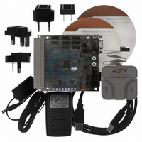
DEV KIT FOR F020/F021/F022/F023
Manufacturer
Silicon Laboratories Inc
Type
MCUr
Datasheet
1.C8051F020DK.pdf
(272 pages)
Specifications of C8051F020DK
Contents
Evaluation Board, Power Supply, USB Cables, Adapter and Documentation
Processor To Be Evaluated
C8051F02x
Interface Type
USB
Silicon Manufacturer
Silicon Labs
Core Architecture
8051
Silicon Core Number
C8051F020
Silicon Family Name
C8051F02x
Lead Free Status / RoHS Status
Contains lead / RoHS non-compliant
For Use With/related Products
Silicon Laboratories C8051 F020/021/022/023
Lead Free Status / Rohs Status
Lead free / RoHS Compliant
Other names
336-1200
Available stocks
Company
Part Number
Manufacturer
Quantity
Price
Company:

Part Number:
C8051F020DK
Manufacturer:
SiliconL
Quantity:
10


C8051F020/1/2/3
Port Data register will cause the Port pin to be driven to GND, and a logic 1 will cause the Port pin to assume a high-
impedance state. The Open-Drain configuration is useful to prevent contention between devices in systems where the
Port pin participates in a shared interconnection in which multiple outputs are connected to the same physical wire.
The output modes of the Port pins on Ports 4 through 7 are determined by the bits in the P74OUT register (see
Figure 17.20). Each bit in P74OUT controls the output mode of a 4-bit bank of Port pins on Ports 4, 5, 6, and 7. A
logic 1 in P74OUT.7 will configure the output modes of 4 most-significant bits of Port 7, P7.[7:4], to Push-Pull; a
logic 0 in P74OUT.7 will configure the output modes of P7.[7:4] to Open-Drain.
17.2.3. Configuring Port Pins as Digital Inputs
A Port pin is configured as a digital input by setting its output mode to “Open-Drain” and writing a logic 1 to the
associated bit in the Port Data register. For example, P7.7 is configured as a digital input by setting P74OUT.7 to a
logic 0 and P7.7 to a logic 1.
17.2.4. Weak Pull-ups
By default, each Port pin has an internal weak pull-up device enabled which provides a resistive connection (about
100 k) between the pin and VDD. The weak pull-up devices can be globally disabled by writing a logic 1 to the
Weak Pull-up Disable bit, (WEAKPUD, XBR2.7). The weak pull-up is automatically deactivated on any pin that is
driving a logic 0; that is, an output pin will not contend with its own pull-up device.
17.2.5. External Memory Interface
If the External Memory Interface (EMIF) is enabled on the High ports (Ports 4 through 7), EMIFLE (XBR2.1) should
be set to a logic 0.
If the External Memory Interface is enabled on the High ports and an off-chip MOVX operation occurs, the External
Memory Interface will control the output states of the affected Port pins during the execution phase of the MOVX
instruction, regardless of the settings of the Port Data registers. The output configuration of the Port pins is not
affected by the EMIF operation, except that Read operations will explicitly disable the output drivers on the Data Bus
during the MOVX execution. See
Section “16. EXTERNAL DATA MEMORY INTERFACE AND ON-CHIP
XRAM” on page 145
for more information about the External Memory Interface.
178
Rev. 1.4
Related parts for C8051F020DK
Image
Part Number
Description
Manufacturer
Datasheet
Request
R

Part Number:
Description:
SMD/C°/SINGLE-ENDED OUTPUT SILICON OSCILLATOR
Manufacturer:
Silicon Laboratories Inc
Part Number:
Description:
Manufacturer:
Silicon Laboratories Inc
Datasheet:
Part Number:
Description:
N/A N/A/SI4010 AES KEYFOB DEMO WITH LCD RX
Manufacturer:
Silicon Laboratories Inc
Datasheet:
Part Number:
Description:
N/A N/A/SI4010 SIMPLIFIED KEY FOB DEMO WITH LED RX
Manufacturer:
Silicon Laboratories Inc
Datasheet:
Part Number:
Description:
N/A/-40 TO 85 OC/EZLINK MODULE; F930/4432 HIGH BAND (REV E/B1)
Manufacturer:
Silicon Laboratories Inc
Part Number:
Description:
EZLink Module; F930/4432 Low Band (rev e/B1)
Manufacturer:
Silicon Laboratories Inc
Part Number:
Description:
I°/4460 10 DBM RADIO TEST CARD 434 MHZ
Manufacturer:
Silicon Laboratories Inc
Part Number:
Description:
I°/4461 14 DBM RADIO TEST CARD 868 MHZ
Manufacturer:
Silicon Laboratories Inc
Part Number:
Description:
I°/4463 20 DBM RFSWITCH RADIO TEST CARD 460 MHZ
Manufacturer:
Silicon Laboratories Inc
Part Number:
Description:
I°/4463 20 DBM RADIO TEST CARD 868 MHZ
Manufacturer:
Silicon Laboratories Inc
Part Number:
Description:
I°/4463 27 DBM RADIO TEST CARD 868 MHZ
Manufacturer:
Silicon Laboratories Inc
Part Number:
Description:
I°/4463 SKYWORKS 30 DBM RADIO TEST CARD 915 MHZ
Manufacturer:
Silicon Laboratories Inc
Part Number:
Description:
N/A N/A/-40 TO 85 OC/4463 RFMD 30 DBM RADIO TEST CARD 915 MHZ
Manufacturer:
Silicon Laboratories Inc
Part Number:
Description:
I°/4463 20 DBM RADIO TEST CARD 169 MHZ
Manufacturer:
Silicon Laboratories Inc