C8051F020DK Silicon Laboratories Inc, C8051F020DK Datasheet - Page 200
C8051F020DK
Manufacturer Part Number
C8051F020DK
Description
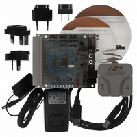
DEV KIT FOR F020/F021/F022/F023
Manufacturer
Silicon Laboratories Inc
Type
MCUr
Datasheet
1.C8051F020DK.pdf
(272 pages)
Specifications of C8051F020DK
Contents
Evaluation Board, Power Supply, USB Cables, Adapter and Documentation
Processor To Be Evaluated
C8051F02x
Interface Type
USB
Silicon Manufacturer
Silicon Labs
Core Architecture
8051
Silicon Core Number
C8051F020
Silicon Family Name
C8051F02x
Lead Free Status / RoHS Status
Contains lead / RoHS non-compliant
For Use With/related Products
Silicon Laboratories C8051 F020/021/022/023
Lead Free Status / Rohs Status
Lead free / RoHS Compliant
Other names
336-1200
Available stocks
Company
Part Number
Manufacturer
Quantity
Price
Company:

Part Number:
C8051F020DK
Manufacturer:
SiliconL
Quantity:
10


C8051F020/1/2/3
Multiple masters may reside on the same bus. A Mode Fault flag (MODF, SPI0CN.5) is set to logic 1 when SPI0 is
configured as a master (MSTEN = 1) and its slave select signal NSS is pulled low. When the Mode Fault flag is set,
the MSTEN and SPIEN bits of the SPI control register are cleared by hardware, thereby placing the SPI0 module in
an "off-line" state. In a multiple-master environment, the system controller should check the state of the SLVSEL flag
(SPI0CN.2) to ensure the bus is free before setting the MSTEN bit and initiating a data transfer.
19.3. Serial Clock Timing
As shown in Figure 19.4, four combinations of serial clock phase and polarity can be selected using the clock control
bits in the SPI0 Configuration Register (SPI0CFG). The CKPHA bit (SPI0CFG.7) selects one of two clock phases
(edge used to latch the data). The CKPOL bit (SPI0CFG.6) selects between an active-high or active-low clock. Both
master and slave devices must be configured to use the same clock phase and polarity. Note: SPI0 should be disabled
(by clearing the SPIEN bit, SPI0CN.0) while changing the clock phase and polarity.
The SPI0 Clock Rate Register (SPI0CKR) as shown in Figure 19.7 controls the master mode serial clock frequency.
This register is ignored when operating in slave mode.
200
SCK
(CKPOL=0, CKPHA=0)
SCK
(CKPOL=0, CKPHA=1)
SCK
(CKPOL=1, CKPHA=0)
SCK
(CKPOL=1, CKPHA=1)
MISO/MOSI
NSS
MSB
Figure 19.4. Data/Clock Timing Diagram
Bit 6
Bit 5
Rev. 1.4
Bit 4
Bit 3
Bit 2
Bit 1
Bit 0
Related parts for C8051F020DK
Image
Part Number
Description
Manufacturer
Datasheet
Request
R

Part Number:
Description:
SMD/C°/SINGLE-ENDED OUTPUT SILICON OSCILLATOR
Manufacturer:
Silicon Laboratories Inc
Part Number:
Description:
Manufacturer:
Silicon Laboratories Inc
Datasheet:
Part Number:
Description:
N/A N/A/SI4010 AES KEYFOB DEMO WITH LCD RX
Manufacturer:
Silicon Laboratories Inc
Datasheet:
Part Number:
Description:
N/A N/A/SI4010 SIMPLIFIED KEY FOB DEMO WITH LED RX
Manufacturer:
Silicon Laboratories Inc
Datasheet:
Part Number:
Description:
N/A/-40 TO 85 OC/EZLINK MODULE; F930/4432 HIGH BAND (REV E/B1)
Manufacturer:
Silicon Laboratories Inc
Part Number:
Description:
EZLink Module; F930/4432 Low Band (rev e/B1)
Manufacturer:
Silicon Laboratories Inc
Part Number:
Description:
I°/4460 10 DBM RADIO TEST CARD 434 MHZ
Manufacturer:
Silicon Laboratories Inc
Part Number:
Description:
I°/4461 14 DBM RADIO TEST CARD 868 MHZ
Manufacturer:
Silicon Laboratories Inc
Part Number:
Description:
I°/4463 20 DBM RFSWITCH RADIO TEST CARD 460 MHZ
Manufacturer:
Silicon Laboratories Inc
Part Number:
Description:
I°/4463 20 DBM RADIO TEST CARD 868 MHZ
Manufacturer:
Silicon Laboratories Inc
Part Number:
Description:
I°/4463 27 DBM RADIO TEST CARD 868 MHZ
Manufacturer:
Silicon Laboratories Inc
Part Number:
Description:
I°/4463 SKYWORKS 30 DBM RADIO TEST CARD 915 MHZ
Manufacturer:
Silicon Laboratories Inc
Part Number:
Description:
N/A N/A/-40 TO 85 OC/4463 RFMD 30 DBM RADIO TEST CARD 915 MHZ
Manufacturer:
Silicon Laboratories Inc
Part Number:
Description:
I°/4463 20 DBM RADIO TEST CARD 169 MHZ
Manufacturer:
Silicon Laboratories Inc