C8051F020DK Silicon Laboratories Inc, C8051F020DK Datasheet - Page 220
C8051F020DK
Manufacturer Part Number
C8051F020DK
Description
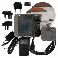
DEV KIT FOR F020/F021/F022/F023
Manufacturer
Silicon Laboratories Inc
Type
MCUr
Datasheet
1.C8051F020DK.pdf
(272 pages)
Specifications of C8051F020DK
Contents
Evaluation Board, Power Supply, USB Cables, Adapter and Documentation
Processor To Be Evaluated
C8051F02x
Interface Type
USB
Silicon Manufacturer
Silicon Labs
Core Architecture
8051
Silicon Core Number
C8051F020
Silicon Family Name
C8051F02x
Lead Free Status / RoHS Status
Contains lead / RoHS non-compliant
For Use With/related Products
Silicon Laboratories C8051 F020/021/022/023
Lead Free Status / Rohs Status
Lead free / RoHS Compliant
Other names
336-1200
Available stocks
Company
Part Number
Manufacturer
Quantity
Price
Company:

Part Number:
C8051F020DK
Manufacturer:
SiliconL
Quantity:
10


C8051F020/1/2/3
21.2. Multiprocessor Communications
Modes 2 and 3 support multiprocessor communication between a master processor and one or more slave processors
by special use of the ninth data bit and the built-in UART1 address recognition hardware. A master processor begins
a transfer with an address byte to select one or more target slave devices. An address byte differs from a data byte in
that its ninth bit is logic 1; in a data byte, the ninth bit is always set to logic 0.
The UART1 address is configured via two SFRs: SADDR1 (Serial Address) and SADEN1 (Serial Address Enable).
SADEN1 sets the bit mask for the address held in SADDR1: bits set to logic 1 in SADEN1 correspond to bits in
SADDR1 that are checked against the received address byte; bits set to logic 0 in SADEN1 correspond to “don’t
care” bits in SADDR1.
Setting the SM21 bit (SCON1.5) configures UART1 such that when a stop bit is received, UART1 will generate an
interrupt only if the ninth bit is logic 1 (RB81 = 1) and the received data byte matches the UART1 slave address. Fol-
lowing the received address interrupt, the slave should clear its SM21 bit to enable interrupts on the reception of the
following data byte(s). Once the entire message is received, the addressed slave should reset its SM21 bit to ignore all
transmissions until it receives the next address byte. While SM21 is logic 1, UART1 ignores all bytes that do not
match the UART1 address and include a ninth bit that is logic 1.
Multiple addresses can be assigned to a single slave and/or a single address can be assigned to multiple slaves,
thereby enabling "broadcast" transmissions to more than one slave simultaneously. The broadcast address is the logi-
cal OR of registers SADDR1 and SADEN1, and ‘0’s of the result are treated as “don’t cares”. Typically a broadcast
address of 0xFF (hexadecimal) is acknowledged by all slaves, assuming “don’t care” bits as ‘1’s. The master proces-
sor can be configured to receive all transmissions or a protocol can be implemented such that the master/slave role is
temporarily reversed to enable half-duplex transmission between the original master and slave(s).
220
UART1 Address = xxxx0101
SADDR1
SADEN1
RX
Example 1
Master
Device
Figure 21.7. UART Multi-Processor Mode Interconnect Diagram
TX
= 00110101
= 00001111
RX
Device
Slave
UART1 Address = 0011xx01
TX
SADDR1
SADEN1
Example 2
Rev. 1.4
RX
Device
Slave
= 00110101
= 11110011
TX
RX
Device
Slave
UART1 Address = 00xxxxxx
SADDR1
SADEN1
TX
Example 3
+5V
= 00110101
= 11000000
Related parts for C8051F020DK
Image
Part Number
Description
Manufacturer
Datasheet
Request
R

Part Number:
Description:
SMD/C°/SINGLE-ENDED OUTPUT SILICON OSCILLATOR
Manufacturer:
Silicon Laboratories Inc
Part Number:
Description:
Manufacturer:
Silicon Laboratories Inc
Datasheet:
Part Number:
Description:
N/A N/A/SI4010 AES KEYFOB DEMO WITH LCD RX
Manufacturer:
Silicon Laboratories Inc
Datasheet:
Part Number:
Description:
N/A N/A/SI4010 SIMPLIFIED KEY FOB DEMO WITH LED RX
Manufacturer:
Silicon Laboratories Inc
Datasheet:
Part Number:
Description:
N/A/-40 TO 85 OC/EZLINK MODULE; F930/4432 HIGH BAND (REV E/B1)
Manufacturer:
Silicon Laboratories Inc
Part Number:
Description:
EZLink Module; F930/4432 Low Band (rev e/B1)
Manufacturer:
Silicon Laboratories Inc
Part Number:
Description:
I°/4460 10 DBM RADIO TEST CARD 434 MHZ
Manufacturer:
Silicon Laboratories Inc
Part Number:
Description:
I°/4461 14 DBM RADIO TEST CARD 868 MHZ
Manufacturer:
Silicon Laboratories Inc
Part Number:
Description:
I°/4463 20 DBM RFSWITCH RADIO TEST CARD 460 MHZ
Manufacturer:
Silicon Laboratories Inc
Part Number:
Description:
I°/4463 20 DBM RADIO TEST CARD 868 MHZ
Manufacturer:
Silicon Laboratories Inc
Part Number:
Description:
I°/4463 27 DBM RADIO TEST CARD 868 MHZ
Manufacturer:
Silicon Laboratories Inc
Part Number:
Description:
I°/4463 SKYWORKS 30 DBM RADIO TEST CARD 915 MHZ
Manufacturer:
Silicon Laboratories Inc
Part Number:
Description:
N/A N/A/-40 TO 85 OC/4463 RFMD 30 DBM RADIO TEST CARD 915 MHZ
Manufacturer:
Silicon Laboratories Inc
Part Number:
Description:
I°/4463 20 DBM RADIO TEST CARD 169 MHZ
Manufacturer:
Silicon Laboratories Inc