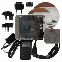
C8051F020DK Silicon Laboratories Inc, C8051F020DK Datasheet - Page 84

C8051F020DK
Manufacturer Part Number
C8051F020DK
Description
DEV KIT FOR F020/F021/F022/F023
Manufacturer
Silicon Laboratories Inc
Type
MCUr
Datasheet
1.C8051F020DK.pdf
(272 pages)
Specifications of C8051F020DK
Contents
Evaluation Board, Power Supply, USB Cables, Adapter and Documentation
Processor To Be Evaluated
C8051F02x
Interface Type
USB
Silicon Manufacturer
Silicon Labs
Core Architecture
8051
Silicon Core Number
C8051F020
Silicon Family Name
C8051F02x
Lead Free Status / RoHS Status
Contains lead / RoHS non-compliant
For Use With/related Products
Silicon Laboratories C8051 F020/021/022/023
Lead Free Status / Rohs Status
Lead free / RoHS Compliant
Other names
336-1200
Available stocks
Company
Part Number
Manufacturer
Quantity
Price
Company:
Part Number:
C8051F020DK
Manufacturer:
SiliconL
Quantity:
10
- Current page: 84 of 272
- Download datasheet (2Mb)
C8051F020/1/2/3
8.1.1. Update Output On-Demand
In its default mode (DAC0CN.[4:3] = ‘00’) the DAC0 output is updated “on-demand” on a write to the high-byte of
the DAC0 data register (DAC0H). It’s important to note that writes to DAC0L are held, and have no effect on the
DAC0 output until a write to DAC0H takes place. If writing a full 12-bit word to the DAC data registers, the 12-bit
data word is written to the low byte (DAC0L) and high byte (DAC0H) data registers. Data is latched into DAC0 after
a write to the corresponding DAC0H register, so the write sequence should be DAC0L followed by DAC0H if the
full 12-bit resolution is required. The DAC can be used in 8-bit mode by initializing DAC0L to the desired value (typ-
ically 0x00), and writing data to only DAC0H (also see
Section 8.2
for information on formatting the 12-bit DAC
data word within the 16-bit SFR space).
8.1.2. Update Output Based on Timer Overflow
Similar to the ADC operation, in which an ADC conversion can be initiated by a timer overflow independently of the
processor, the DAC outputs can use a Timer overflow to schedule an output update event. This feature is useful in
systems where the DAC is used to generate a waveform of a defined sampling rate by eliminating the effects of vari-
able interrupt latency and instruction execution on the timing of the DAC output. When the DAC0MD bits
(DAC0CN.[4:3]) are set to ‘01’, ‘10’, or ‘11’, writes to both DAC data registers (DAC0L and DAC0H) are held until
an associated Timer overflow event (Timer 3, Timer 4, or Timer 2, respectively) occurs, at which time the
DAC0H:DAC0L contents are copied to the DAC input latches allowing the DAC output to change to the new value.
8.2.
DAC Output Scaling/Justification
In some instances, input data should be shifted prior to a DAC0 write operation to properly justify data within the
DAC input registers. This action would typically require one or more load and shift operations, adding software over-
head and slowing DAC throughput. To alleviate this problem, the data-formatting feature provides a means for the
user to program the orientation of the DAC0 data word within data registers DAC0H and DAC0L. The three
DAC0DF bits (DAC0CN.[2:0]) allow the user to specify one of five data word orientations as shown in the DAC0CN
register definition.
DAC1 is functionally the same as DAC0 described above. The electrical specifications for both DAC0 and DAC1 are
given in Table 8.1.
84
Rev. 1.4
Related parts for C8051F020DK
Image
Part Number
Description
Manufacturer
Datasheet
Request
R
Part Number:
Description:
SMD/C°/SINGLE-ENDED OUTPUT SILICON OSCILLATOR
Manufacturer:
Silicon Laboratories Inc
Part Number:
Description:
Manufacturer:
Silicon Laboratories Inc
Datasheet:
Part Number:
Description:
N/A N/A/SI4010 AES KEYFOB DEMO WITH LCD RX
Manufacturer:
Silicon Laboratories Inc
Datasheet:
Part Number:
Description:
N/A N/A/SI4010 SIMPLIFIED KEY FOB DEMO WITH LED RX
Manufacturer:
Silicon Laboratories Inc
Datasheet:
Part Number:
Description:
N/A/-40 TO 85 OC/EZLINK MODULE; F930/4432 HIGH BAND (REV E/B1)
Manufacturer:
Silicon Laboratories Inc
Part Number:
Description:
EZLink Module; F930/4432 Low Band (rev e/B1)
Manufacturer:
Silicon Laboratories Inc
Part Number:
Description:
I°/4460 10 DBM RADIO TEST CARD 434 MHZ
Manufacturer:
Silicon Laboratories Inc
Part Number:
Description:
I°/4461 14 DBM RADIO TEST CARD 868 MHZ
Manufacturer:
Silicon Laboratories Inc
Part Number:
Description:
I°/4463 20 DBM RFSWITCH RADIO TEST CARD 460 MHZ
Manufacturer:
Silicon Laboratories Inc
Part Number:
Description:
I°/4463 20 DBM RADIO TEST CARD 868 MHZ
Manufacturer:
Silicon Laboratories Inc
Part Number:
Description:
I°/4463 27 DBM RADIO TEST CARD 868 MHZ
Manufacturer:
Silicon Laboratories Inc
Part Number:
Description:
I°/4463 SKYWORKS 30 DBM RADIO TEST CARD 915 MHZ
Manufacturer:
Silicon Laboratories Inc
Part Number:
Description:
N/A N/A/-40 TO 85 OC/4463 RFMD 30 DBM RADIO TEST CARD 915 MHZ
Manufacturer:
Silicon Laboratories Inc
Part Number:
Description:
I°/4463 20 DBM RADIO TEST CARD 169 MHZ
Manufacturer:
Silicon Laboratories Inc


