C8051F410DK Silicon Laboratories Inc, C8051F410DK Datasheet - Page 129
C8051F410DK
Manufacturer Part Number
C8051F410DK
Description
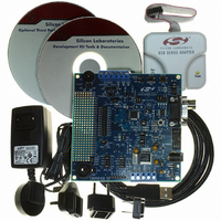
KIT DEV FOR C8051F41X
Manufacturer
Silicon Laboratories Inc
Type
MCUr
Specifications of C8051F410DK
Contents
Evaluation Board, Power Supply, USB Cables, Adapter and Documentation
Processor To Be Evaluated
C8051F41x
Interface Type
USB
Silicon Manufacturer
Silicon Labs
Core Architecture
8051
Silicon Core Number
C8051F410
Silicon Family Name
C8051F41x
Lead Free Status / RoHS Status
Contains lead / RoHS non-compliant
For Use With/related Products
Silicon Laboratories C8051F41x
Lead Free Status / Rohs Status
Lead free / RoHS Compliant
Other names
336-1314
Available stocks
Company
Part Number
Manufacturer
Quantity
Price
Company:

Part Number:
C8051F410DK
Manufacturer:
Silicon Labs
Quantity:
135


15.2. Power-Fail Reset / V
When the VDD Monitor is selected as a reset source and a power-down transition or power irregularity
causes V
in a reset state (see Figure 15.2). When V
from the reset state. Note that even though internal data memory contents are not altered by the power-fail
reset, it is impossible to determine if V
flag reads ‘1’, the data may no longer be valid. The V
source after power-on resets; however its defined state (enabled/disabled) is not altered by any other reset
source. For example, if the V
V
monitor must be enabled to the higher setting (VDMLVL = '1') and selected as a reset source if soft-
ware contains routines which erase or write Flash memory. If the V
erase or write performed on Flash memory will cause a Flash Error device reset.
The V
as a reset source before it is enabled and stabilized may cause a system reset. The procedure for re-
enabling the V
See Figure 15.2 for V
See Table 15.1 for complete electrical characteristics of the V
Note: Software should take care not to inadvertently disable the V
when writing to RSTSRC to enable other reset sources or to trigger a software reset. All writes to
RSTSRC should explicitly set PORSF to '1' to keep the V
DD
monitor will still be disabled after the reset. To protect the integrity of Flash contents, the V
DD
Step 1. Enable the V
Step 2. Wait for the V
Step 3. Select the V
DD
monitor must be enabled before it is selected as a reset source. Selecting the V
to drop below V
DD
Note: This delay should be omitted if software contains routines which erase or
write Flash memory.
monitor and configuring the V
DD
monitor timing; note that the reset delay is not incurred after a V
RST
DD
DD
DD
DD
, the power supply monitor will drive the RST pin low and hold the CIP-51
monitor as a reset source (PORSF bit in RSTSRC = ‘1’).
monitor (VDMEN bit in VDM0CN = ‘1’).
monitor is disabled by software, and a software reset is performed, the
monitor to stabilize (approximately 5 µs).
DD
DD
Monitor
dropped below the level required for data retention. If the PORSF
DD
returns to a level above V
DD
Rev. 1.1
monitor as a reset source is shown below:
DD
monitor is enabled and is selected as a reset
DD
DD
Monitor enabled as a reset source.
monitor.
C8051F410/1/2/3
DD
RST
DD
monitor is not enabled, any
, the CIP-51 will be released
Monitor as a reset source
DD
monitor reset.
DD
monitor
129
DD
Related parts for C8051F410DK
Image
Part Number
Description
Manufacturer
Datasheet
Request
R

Part Number:
Description:
SMD/C°/SINGLE-ENDED OUTPUT SILICON OSCILLATOR
Manufacturer:
Silicon Laboratories Inc
Part Number:
Description:
Manufacturer:
Silicon Laboratories Inc
Datasheet:
Part Number:
Description:
N/A N/A/SI4010 AES KEYFOB DEMO WITH LCD RX
Manufacturer:
Silicon Laboratories Inc
Datasheet:
Part Number:
Description:
N/A N/A/SI4010 SIMPLIFIED KEY FOB DEMO WITH LED RX
Manufacturer:
Silicon Laboratories Inc
Datasheet:
Part Number:
Description:
N/A/-40 TO 85 OC/EZLINK MODULE; F930/4432 HIGH BAND (REV E/B1)
Manufacturer:
Silicon Laboratories Inc
Part Number:
Description:
EZLink Module; F930/4432 Low Band (rev e/B1)
Manufacturer:
Silicon Laboratories Inc
Part Number:
Description:
I°/4460 10 DBM RADIO TEST CARD 434 MHZ
Manufacturer:
Silicon Laboratories Inc
Part Number:
Description:
I°/4461 14 DBM RADIO TEST CARD 868 MHZ
Manufacturer:
Silicon Laboratories Inc
Part Number:
Description:
I°/4463 20 DBM RFSWITCH RADIO TEST CARD 460 MHZ
Manufacturer:
Silicon Laboratories Inc
Part Number:
Description:
I°/4463 20 DBM RADIO TEST CARD 868 MHZ
Manufacturer:
Silicon Laboratories Inc
Part Number:
Description:
I°/4463 27 DBM RADIO TEST CARD 868 MHZ
Manufacturer:
Silicon Laboratories Inc
Part Number:
Description:
I°/4463 SKYWORKS 30 DBM RADIO TEST CARD 915 MHZ
Manufacturer:
Silicon Laboratories Inc
Part Number:
Description:
N/A N/A/-40 TO 85 OC/4463 RFMD 30 DBM RADIO TEST CARD 915 MHZ
Manufacturer:
Silicon Laboratories Inc
Part Number:
Description:
I°/4463 20 DBM RADIO TEST CARD 169 MHZ
Manufacturer:
Silicon Laboratories Inc