C8051F410DK Silicon Laboratories Inc, C8051F410DK Datasheet - Page 195
C8051F410DK
Manufacturer Part Number
C8051F410DK
Description
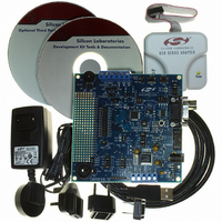
KIT DEV FOR C8051F41X
Manufacturer
Silicon Laboratories Inc
Type
MCUr
Specifications of C8051F410DK
Contents
Evaluation Board, Power Supply, USB Cables, Adapter and Documentation
Processor To Be Evaluated
C8051F41x
Interface Type
USB
Silicon Manufacturer
Silicon Labs
Core Architecture
8051
Silicon Core Number
C8051F410
Silicon Family Name
C8051F41x
Lead Free Status / RoHS Status
Contains lead / RoHS non-compliant
For Use With/related Products
Silicon Laboratories C8051F41x
Lead Free Status / Rohs Status
Lead free / RoHS Compliant
Other names
336-1314
Available stocks
Company
Part Number
Manufacturer
Quantity
Price
Company:

Part Number:
C8051F410DK
Manufacturer:
Silicon Labs
Quantity:
135


SMBus configuration options include:
•
•
•
•
These options are selected in the SMB0CF register, as described in
tion Register” on page 195
21.4.1. SMBus Configuration Register
The SMBus Configuration register (SMB0CF) is used to enable the SMBus Master and/or Slave modes,
select the SMBus clock source, and select the SMBus timing and timeout options. When the ENSMB bit is
set, the SMBus is enabled for all master and slave events. Slave events may be disabled by setting the
INH bit. With slave events inhibited, the SMBus interface will still monitor the SCL and SDA pins; however,
the interface will NACK all received addresses and will not generate any slave interrupts. When the INH bit
is set, all slave events will be inhibited following the next START (interrupts will continue for the duration of
the current transfer).
The SMBCS1-0 bits select the SMBus clock source, which is used only when operating as a master or
when the Bus Free Timeout detection is enabled. When operating as a master, overflows from the selected
source determine the absolute minimum SCL low and high times as defined in Equation 21.1. Note that the
selected clock source may be shared by other peripherals so long as the timer is left running at all times.
For example, Timer 1 overflows may generate the SMBus and UART baud rates simultaneously. Timer
configuration is covered in
The selected clock source should be configured to establish the minimum SCL High and Low times as per
Equation 21.1. When the interface is operating as a master (and SCL is not driven or extended by any
other devices on the bus), the typical SMBus bit rate is approximated by Equation 21.2.
Timeout detection (SCL Low Timeout and/or Bus Free Timeout)
SDA setup and hold time extensions
Slave event enable/disable
Clock source selection
Equation 21.1. Minimum SCL High and Low Times
Table 21.1. SMBus Clock Source Selection
SMBCS1 SMBCS0
Section “24. Timers” on page 231
T
Equation 21.2. Typical SMBus Bit Rate
HighMin
.
0
0
1
1
BitRate
=
T
0
1
0
1
LowMin
=
f
--------------------------------------------- -
ClockSourceOverflow
Rev. 1.1
Timer 2 High Byte Overflow
Timer 2 Low Byte Overflow
=
SMBus Clock Source
--------------------------------------------- -
f
ClockSourceOverflow
Timer 0 Overflow
Timer 1 Overflow
3
.
1
Section “21.4.1. SMBus Configura-
C8051F410/1/2/3
195
Related parts for C8051F410DK
Image
Part Number
Description
Manufacturer
Datasheet
Request
R

Part Number:
Description:
SMD/C°/SINGLE-ENDED OUTPUT SILICON OSCILLATOR
Manufacturer:
Silicon Laboratories Inc
Part Number:
Description:
Manufacturer:
Silicon Laboratories Inc
Datasheet:
Part Number:
Description:
N/A N/A/SI4010 AES KEYFOB DEMO WITH LCD RX
Manufacturer:
Silicon Laboratories Inc
Datasheet:
Part Number:
Description:
N/A N/A/SI4010 SIMPLIFIED KEY FOB DEMO WITH LED RX
Manufacturer:
Silicon Laboratories Inc
Datasheet:
Part Number:
Description:
N/A/-40 TO 85 OC/EZLINK MODULE; F930/4432 HIGH BAND (REV E/B1)
Manufacturer:
Silicon Laboratories Inc
Part Number:
Description:
EZLink Module; F930/4432 Low Band (rev e/B1)
Manufacturer:
Silicon Laboratories Inc
Part Number:
Description:
I°/4460 10 DBM RADIO TEST CARD 434 MHZ
Manufacturer:
Silicon Laboratories Inc
Part Number:
Description:
I°/4461 14 DBM RADIO TEST CARD 868 MHZ
Manufacturer:
Silicon Laboratories Inc
Part Number:
Description:
I°/4463 20 DBM RFSWITCH RADIO TEST CARD 460 MHZ
Manufacturer:
Silicon Laboratories Inc
Part Number:
Description:
I°/4463 20 DBM RADIO TEST CARD 868 MHZ
Manufacturer:
Silicon Laboratories Inc
Part Number:
Description:
I°/4463 27 DBM RADIO TEST CARD 868 MHZ
Manufacturer:
Silicon Laboratories Inc
Part Number:
Description:
I°/4463 SKYWORKS 30 DBM RADIO TEST CARD 915 MHZ
Manufacturer:
Silicon Laboratories Inc
Part Number:
Description:
N/A N/A/-40 TO 85 OC/4463 RFMD 30 DBM RADIO TEST CARD 915 MHZ
Manufacturer:
Silicon Laboratories Inc
Part Number:
Description:
I°/4463 20 DBM RADIO TEST CARD 169 MHZ
Manufacturer:
Silicon Laboratories Inc