C8051F410DK Silicon Laboratories Inc, C8051F410DK Datasheet - Page 220
C8051F410DK
Manufacturer Part Number
C8051F410DK
Description
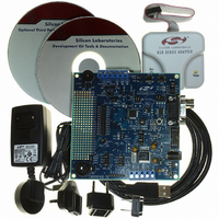
KIT DEV FOR C8051F41X
Manufacturer
Silicon Laboratories Inc
Type
MCUr
Specifications of C8051F410DK
Contents
Evaluation Board, Power Supply, USB Cables, Adapter and Documentation
Processor To Be Evaluated
C8051F41x
Interface Type
USB
Silicon Manufacturer
Silicon Labs
Core Architecture
8051
Silicon Core Number
C8051F410
Silicon Family Name
C8051F41x
Lead Free Status / RoHS Status
Contains lead / RoHS non-compliant
For Use With/related Products
Silicon Laboratories C8051F41x
Lead Free Status / Rohs Status
Lead free / RoHS Compliant
Other names
336-1314
Available stocks
Company
Part Number
Manufacturer
Quantity
Price
Company:

Part Number:
C8051F410DK
Manufacturer:
Silicon Labs
Quantity:
135


C8051F410/1/2/3
23.3. SPI0 Slave Mode Operation
When SPI0 is enabled and not configured as a master, it will operate as a SPI slave. As a slave, bytes are
shifted in through the MOSI pin and out through the MISO pin by a master device controlling the SCK sig-
nal. A bit counter in the SPI0 logic counts SCK edges. When 8 bits have been shifted into the shift register,
the SPIF flag is set to logic 1, and the byte is copied into the receive buffer. Data is read from the receive
buffer by reading SPI0DAT. A slave device cannot initiate transfers. Data to be transferred to the master
device is pre-loaded into the shift register by writing to SPI0DAT. Writes to SPI0DAT are double-buffered,
and are placed in the transmit buffer first. If the shift register is empty, the contents of the transmit buffer
will immediately be transferred into the shift register. When the shift register already contains data, the SPI
will load the shift register with the transmit buffer’s contents after the last SCK edge of the next (or current)
SPI transfer.
220
Figure 23.3. 3-Wire Single Master and Slave Mode Connection Diagram
Figure 23.4. 4-Wire Single Master and Slave Mode Connection Diagram
Figure 23.2. Multiple-Master Mode Connection Diagram
Device 1
Master
Master
Device
Master
Device
GPIO
MISO
MOSI
GPIO
MISO
MOSI
MISO
MOSI
NSS
SCK
SCK
SCK
NSS
Rev. 1.1
GPIO
MISO
MOSI
SCK
NSS
MISO
MOSI
SCK
MISO
MOSI
SCK
NSS
MISO
MOSI
SCK
NSS
Device 2
Master
Device
Device
Device
Slave
Slave
Slave
Related parts for C8051F410DK
Image
Part Number
Description
Manufacturer
Datasheet
Request
R

Part Number:
Description:
SMD/C°/SINGLE-ENDED OUTPUT SILICON OSCILLATOR
Manufacturer:
Silicon Laboratories Inc
Part Number:
Description:
Manufacturer:
Silicon Laboratories Inc
Datasheet:
Part Number:
Description:
N/A N/A/SI4010 AES KEYFOB DEMO WITH LCD RX
Manufacturer:
Silicon Laboratories Inc
Datasheet:
Part Number:
Description:
N/A N/A/SI4010 SIMPLIFIED KEY FOB DEMO WITH LED RX
Manufacturer:
Silicon Laboratories Inc
Datasheet:
Part Number:
Description:
N/A/-40 TO 85 OC/EZLINK MODULE; F930/4432 HIGH BAND (REV E/B1)
Manufacturer:
Silicon Laboratories Inc
Part Number:
Description:
EZLink Module; F930/4432 Low Band (rev e/B1)
Manufacturer:
Silicon Laboratories Inc
Part Number:
Description:
I°/4460 10 DBM RADIO TEST CARD 434 MHZ
Manufacturer:
Silicon Laboratories Inc
Part Number:
Description:
I°/4461 14 DBM RADIO TEST CARD 868 MHZ
Manufacturer:
Silicon Laboratories Inc
Part Number:
Description:
I°/4463 20 DBM RFSWITCH RADIO TEST CARD 460 MHZ
Manufacturer:
Silicon Laboratories Inc
Part Number:
Description:
I°/4463 20 DBM RADIO TEST CARD 868 MHZ
Manufacturer:
Silicon Laboratories Inc
Part Number:
Description:
I°/4463 27 DBM RADIO TEST CARD 868 MHZ
Manufacturer:
Silicon Laboratories Inc
Part Number:
Description:
I°/4463 SKYWORKS 30 DBM RADIO TEST CARD 915 MHZ
Manufacturer:
Silicon Laboratories Inc
Part Number:
Description:
N/A N/A/-40 TO 85 OC/4463 RFMD 30 DBM RADIO TEST CARD 915 MHZ
Manufacturer:
Silicon Laboratories Inc
Part Number:
Description:
I°/4463 20 DBM RADIO TEST CARD 169 MHZ
Manufacturer:
Silicon Laboratories Inc