C8051F410DK Silicon Laboratories Inc, C8051F410DK Datasheet - Page 268
C8051F410DK
Manufacturer Part Number
C8051F410DK
Description
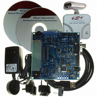
KIT DEV FOR C8051F41X
Manufacturer
Silicon Laboratories Inc
Type
MCUr
Specifications of C8051F410DK
Contents
Evaluation Board, Power Supply, USB Cables, Adapter and Documentation
Processor To Be Evaluated
C8051F41x
Interface Type
USB
Silicon Manufacturer
Silicon Labs
Core Architecture
8051
Silicon Core Number
C8051F410
Silicon Family Name
C8051F41x
Lead Free Status / RoHS Status
Contains lead / RoHS non-compliant
For Use With/related Products
Silicon Laboratories C8051F41x
Lead Free Status / Rohs Status
Lead free / RoHS Compliant
Other names
336-1314
Available stocks
Company
Part Number
Manufacturer
Quantity
Price
Company:

Part Number:
C8051F410DK
Manufacturer:
Silicon Labs
Quantity:
135


C8051F410/1/2/3
D
Revision 0.7 to Revision 0.8
•
•
•
•
•
•
•
•
•
•
•
•
•
•
•
Revision 0.8 to Revision 1.0
•
•
•
•
•
•
Revision 1.0 to Revision 1.1
•
•
•
•
•
•
268
OCUMENT
Updated specification tables with most recently available characterization data.
Corrected references to configuring pins for Analog Mode - Port Latch must contain a '1'.
SFR Definition 5.6: Address correction to 0xBA.
Added Figure 8.2 showing power connection diagram without using on-chip regulator.
Section 9
Table 11.2 : Corrected SFR Name P2MDIN on location 0xF3.
Section 14
Section 18
last sentence.
Section 19.2.2
Section 19.3
cies.
Section 21
Table 21.4 : Made corrections to SMBus state descriptions.
Figure 24.6 : Corrected T2RCLK Mux selection options.
Figure 24.9 : Corrected T3RCLK Mux selection options.
C2 Register Definition 26.2 : Corrected DEVICEID value to 0x0C.
Updated specification tables with full characterization data.
Updated Flash write and erase procedures to include a write to FLSCL.3-0.
Changed /RST pin comments in Table 4.1, “Pin Definitions for the C8051F41x,” on page 41 for the recom-
mended pull-up resistor.
Changed the reset value of the SFR Definition 16.3. FLSCL: Flash Scale.
Removed the "Optional GND Connection" from Figure 4.5. ’Typical QFN-28 Landing Diagram’ on page 48.
Added a note regarding the maximum SYSCLK frequency to SFR Definition 19.4. CLKMUL: Clock Multi-
plier Control.
Updated Figure 4.3. ’LQFP-32 Package Diagram’ on page 46, Figure 4.5. ’QFN-28 Package Drawing’ on
page 48, and Figure 4.6. ’QFN-28 Recommended PCB Land Pattern’ on page 49.
Added note that VIO must be > VDD in Table 3.1, “Global DC Electrical Characteristics,” on page 36.
Added information about ADC0 output register auto-clearing in SFR Definition 5.2.
Corrected ADC0 Tracking time equation in SFR Definition 5.6.
Clarified Voltage Regulator Electrical Specifications in Table 8.1 on page 82.
Added information about 16-bit and 32-bit CRC algorithms in
: Removed references to "High Speed Analog Mode".
, Important Note on page 151 : Added "and have the same behavior as P0 in Normal Mode." to
: Corrected SMBus maximum rate to 1/20th system clock.
: Corrected operational description of CRC engine.
: Added Figure 19.3 and text to describe behavior of clock multiplier with slower input frequen-
C
: Inserted Step 3 "Release the crystal pins by writing ‘1's to the port latch."
HANGE
L
IST
Rev. 1.1
Section 14
.
Related parts for C8051F410DK
Image
Part Number
Description
Manufacturer
Datasheet
Request
R

Part Number:
Description:
SMD/C°/SINGLE-ENDED OUTPUT SILICON OSCILLATOR
Manufacturer:
Silicon Laboratories Inc
Part Number:
Description:
Manufacturer:
Silicon Laboratories Inc
Datasheet:
Part Number:
Description:
N/A N/A/SI4010 AES KEYFOB DEMO WITH LCD RX
Manufacturer:
Silicon Laboratories Inc
Datasheet:
Part Number:
Description:
N/A N/A/SI4010 SIMPLIFIED KEY FOB DEMO WITH LED RX
Manufacturer:
Silicon Laboratories Inc
Datasheet:
Part Number:
Description:
N/A/-40 TO 85 OC/EZLINK MODULE; F930/4432 HIGH BAND (REV E/B1)
Manufacturer:
Silicon Laboratories Inc
Part Number:
Description:
EZLink Module; F930/4432 Low Band (rev e/B1)
Manufacturer:
Silicon Laboratories Inc
Part Number:
Description:
I°/4460 10 DBM RADIO TEST CARD 434 MHZ
Manufacturer:
Silicon Laboratories Inc
Part Number:
Description:
I°/4461 14 DBM RADIO TEST CARD 868 MHZ
Manufacturer:
Silicon Laboratories Inc
Part Number:
Description:
I°/4463 20 DBM RFSWITCH RADIO TEST CARD 460 MHZ
Manufacturer:
Silicon Laboratories Inc
Part Number:
Description:
I°/4463 20 DBM RADIO TEST CARD 868 MHZ
Manufacturer:
Silicon Laboratories Inc
Part Number:
Description:
I°/4463 27 DBM RADIO TEST CARD 868 MHZ
Manufacturer:
Silicon Laboratories Inc
Part Number:
Description:
I°/4463 SKYWORKS 30 DBM RADIO TEST CARD 915 MHZ
Manufacturer:
Silicon Laboratories Inc
Part Number:
Description:
N/A N/A/-40 TO 85 OC/4463 RFMD 30 DBM RADIO TEST CARD 915 MHZ
Manufacturer:
Silicon Laboratories Inc
Part Number:
Description:
I°/4463 20 DBM RADIO TEST CARD 169 MHZ
Manufacturer:
Silicon Laboratories Inc