C8051F410DK Silicon Laboratories Inc, C8051F410DK Datasheet - Page 3
C8051F410DK
Manufacturer Part Number
C8051F410DK
Description
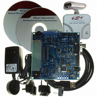
KIT DEV FOR C8051F41X
Manufacturer
Silicon Laboratories Inc
Type
MCUr
Specifications of C8051F410DK
Contents
Evaluation Board, Power Supply, USB Cables, Adapter and Documentation
Processor To Be Evaluated
C8051F41x
Interface Type
USB
Silicon Manufacturer
Silicon Labs
Core Architecture
8051
Silicon Core Number
C8051F410
Silicon Family Name
C8051F41x
Lead Free Status / RoHS Status
Contains lead / RoHS non-compliant
For Use With/related Products
Silicon Laboratories C8051F41x
Lead Free Status / Rohs Status
Lead free / RoHS Compliant
Other names
336-1314
Available stocks
Company
Part Number
Manufacturer
Quantity
Price
Company:

Part Number:
C8051F410DK
Manufacturer:
Silicon Labs
Quantity:
135


Table of Contents
1. System Overview.................................................................................................... 19
2. Absolute Maximum Ratings .................................................................................. 35
3. Global DC Electrical Characteristics .................................................................... 36
4. Pinout and Package Definitions............................................................................ 41
5. 12-Bit ADC (ADC0).................................................................................................. 51
6. 12-Bit Current Mode DACs (IDA0 and IDA1) ........................................................ 69
7. Voltage Reference .................................................................................................. 77
8. Voltage Regulator (REG0)...................................................................................... 81
9. Comparators ......................................................................................................... 83
1.1. CIP-51™ Microcontroller................................................................................... 25
1.2. On-Chip Debug Circuitry................................................................................... 26
1.3. On-Chip Memory............................................................................................... 27
1.4. Operating Modes .............................................................................................. 28
1.5. 12-Bit Analog to Digital Converter..................................................................... 29
1.6. Two 12-bit Current-Mode DACs........................................................................ 29
1.7. Programmable Comparators............................................................................. 30
1.8. Cyclic Redundancy Check Unit......................................................................... 31
1.9. Voltage Regulator ............................................................................................. 31
1.10.Serial Ports ....................................................................................................... 31
1.11.smaRTClock (Real Time Clock) ....................................................................... 32
1.12.Port Input/Output .............................................................................................. 33
1.13.Programmable Counter Array........................................................................... 34
5.1. Analog Multiplexer ............................................................................................ 51
5.2. Temperature Sensor ......................................................................................... 52
5.3. ADC0 Operation................................................................................................ 52
5.4. Programmable Window Detector ...................................................................... 63
6.1. IDAC Output Scheduling................................................................................... 69
6.2. IDAC Output Mapping....................................................................................... 70
6.3. IDAC External Pin Connections ........................................................................ 73
1.1.1. Fully 8051 Compatible Instruction Set...................................................... 25
1.1.2. Improved Throughput ............................................................................... 25
1.1.3. Additional Features .................................................................................. 25
5.3.1. Starting a Conversion............................................................................... 53
5.3.2. Tracking Modes........................................................................................ 53
5.3.3. Timing....................................................................................................... 54
5.3.4. Burst Mode ............................................................................................... 56
5.3.5. Output Conversion Code.......................................................................... 57
5.3.6. Settling Time Requirements ..................................................................... 58
5.4.1. Window Detector In Single-Ended Mode ................................................. 66
6.1.1. Update Output On-Demand ..................................................................... 69
6.1.2. Update Output Based on Timer Overflow ................................................ 70
6.1.3. Update Output Based on CNVSTR Edge................................................. 70
Rev. 1.1
C8051F410/1/2/3
3
Related parts for C8051F410DK
Image
Part Number
Description
Manufacturer
Datasheet
Request
R

Part Number:
Description:
SMD/C°/SINGLE-ENDED OUTPUT SILICON OSCILLATOR
Manufacturer:
Silicon Laboratories Inc
Part Number:
Description:
Manufacturer:
Silicon Laboratories Inc
Datasheet:
Part Number:
Description:
N/A N/A/SI4010 AES KEYFOB DEMO WITH LCD RX
Manufacturer:
Silicon Laboratories Inc
Datasheet:
Part Number:
Description:
N/A N/A/SI4010 SIMPLIFIED KEY FOB DEMO WITH LED RX
Manufacturer:
Silicon Laboratories Inc
Datasheet:
Part Number:
Description:
N/A/-40 TO 85 OC/EZLINK MODULE; F930/4432 HIGH BAND (REV E/B1)
Manufacturer:
Silicon Laboratories Inc
Part Number:
Description:
EZLink Module; F930/4432 Low Band (rev e/B1)
Manufacturer:
Silicon Laboratories Inc
Part Number:
Description:
I°/4460 10 DBM RADIO TEST CARD 434 MHZ
Manufacturer:
Silicon Laboratories Inc
Part Number:
Description:
I°/4461 14 DBM RADIO TEST CARD 868 MHZ
Manufacturer:
Silicon Laboratories Inc
Part Number:
Description:
I°/4463 20 DBM RFSWITCH RADIO TEST CARD 460 MHZ
Manufacturer:
Silicon Laboratories Inc
Part Number:
Description:
I°/4463 20 DBM RADIO TEST CARD 868 MHZ
Manufacturer:
Silicon Laboratories Inc
Part Number:
Description:
I°/4463 27 DBM RADIO TEST CARD 868 MHZ
Manufacturer:
Silicon Laboratories Inc
Part Number:
Description:
I°/4463 SKYWORKS 30 DBM RADIO TEST CARD 915 MHZ
Manufacturer:
Silicon Laboratories Inc
Part Number:
Description:
N/A N/A/-40 TO 85 OC/4463 RFMD 30 DBM RADIO TEST CARD 915 MHZ
Manufacturer:
Silicon Laboratories Inc
Part Number:
Description:
I°/4463 20 DBM RADIO TEST CARD 169 MHZ
Manufacturer:
Silicon Laboratories Inc