C8051F410DK Silicon Laboratories Inc, C8051F410DK Datasheet - Page 36
C8051F410DK
Manufacturer Part Number
C8051F410DK
Description
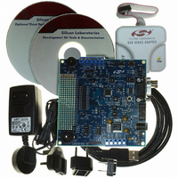
KIT DEV FOR C8051F41X
Manufacturer
Silicon Laboratories Inc
Type
MCUr
Specifications of C8051F410DK
Contents
Evaluation Board, Power Supply, USB Cables, Adapter and Documentation
Processor To Be Evaluated
C8051F41x
Interface Type
USB
Silicon Manufacturer
Silicon Labs
Core Architecture
8051
Silicon Core Number
C8051F410
Silicon Family Name
C8051F41x
Lead Free Status / RoHS Status
Contains lead / RoHS non-compliant
For Use With/related Products
Silicon Laboratories C8051F41x
Lead Free Status / Rohs Status
Lead free / RoHS Compliant
Other names
336-1314
Available stocks
Company
Part Number
Manufacturer
Quantity
Price
Company:

Part Number:
C8051F410DK
Manufacturer:
Silicon Labs
Quantity:
135


C8051F410/1/2/3
3.
Table 3.1. Global DC Electrical Characteristics
–40 to +85 °C, 50 MHz System Clock unless otherwise specified. Typical values are given at 25 °C
36
Supply Input Voltage (V
Core Supply Voltage (V
I/O Supply Voltage (V
Backup Supply Voltage (V
Backup Supply Current
(I
(V
Core Supply RAM Data Retention Voltage
SYSCLK (System Clock)
Specified Operating Temperature Range
Notes:
RTC-BACKUP
DD
1. For more information on V
2.
3. The Backup Supply Voltage (V
4. SYSCLK is the internal device clock. For operational speeds in excess of 25 MHz, SYSCLK must
5. SYSCLK must be at least 32 kHz to enable debugging.
6. Based on device characterization data, not production tested.
7. Active and Inactive IDD at voltages and frequencies other than those specified can be calculated
8. I
9. Idle IDD can be estimated for frequencies < 1 MHz by simply multiplying the frequency of interest by
= 0 V, smaRTClock clock = 32 kHz)
Global DC Electrical Characteristics
VIO must be equal to or greater than VDD.
be derived from the internal clock multiplier.
using the IDD Supply Sensitivity. For example, if the V
I
(2.2 V – 2.0 V) = 5.73 mA at 2.2 V and f = 25 MHz.
frequency sensitivity number for that range. When using these numbers to estimate I
15 MHz, the estimate should be the current at 25 MHz minus the difference in current indicated by
the frequency sensitivity number. For example: V
I
the frequency sensitivity number for that range. When using these numbers to estimate Idle for >
1 MHz, the estimate should be the current at 25 MHz minus the difference in current indicated by
the frequency sensitivity number. For example: V
I
DD
DD
DD
DD
= 5.5 mA typical at 2.0 V and f = 25 MHz. From this, I
can be estimated for frequencies < 15 MHz by simply multiplying the frequency of interest by the
= 5.5 mA – (25 MHz – 20 MHz) x 0.16 mA/MHz = 4.7 mA.
= 2.8 mA – (25 MHz – 5 MHz) x 0.1 mA/MHz = 0.8 mA.
)
Parameter
IO
DD
)
REGIN
2
4,5
)
RTC-BACKUP
)
1
REGIN
RTC-BACKUP
)
3
characteristics, see Table 8.1 on page 82.
Output Current = 1 mA
V
V
V
RTC-BACKUP
RTC-BACKUP
RTC-BACKUP
at –40 ºC
at 25 ºC
at 85 ºC
at –40 ºC
at 25 ºC
at 85 ºC
at –40 ºC
at 25 ºC
at 85 ºC
Rev. 1.1
) is used to power the smaRTClock peripheral only.
Conditions
DD
DD
= 1.0 V:
= 1.8 V:
= 2.5 V:
= 2.0 V; F = 20 MHz,
= 2.0 V; F = 5 MHz, Idle
DD
DD
is 2.2 V instead of 2.0 V at 25 MHz:
= 5.5 mA + 1.14 x
2.15
Min
–40
2.0
2.0
1.0
—
—
—
—
—
—
—
—
—
—
0
0.65
0.92
1.45
0.72
0.95
Typ
0.9
1.4
0.7
1.5
1.5
—
—
—
—
—
—
Max
5.25
2.75
5.25
5.25
1.85
+85
1.5
1.8
2.5
1.6
2.6
50
—
—
—
—
DD
for >
Units
MHz
µA
µA
µA
µA
µA
µA
µA
µA
µA
°C
V
V
V
V
V
Related parts for C8051F410DK
Image
Part Number
Description
Manufacturer
Datasheet
Request
R

Part Number:
Description:
SMD/C°/SINGLE-ENDED OUTPUT SILICON OSCILLATOR
Manufacturer:
Silicon Laboratories Inc
Part Number:
Description:
Manufacturer:
Silicon Laboratories Inc
Datasheet:
Part Number:
Description:
N/A N/A/SI4010 AES KEYFOB DEMO WITH LCD RX
Manufacturer:
Silicon Laboratories Inc
Datasheet:
Part Number:
Description:
N/A N/A/SI4010 SIMPLIFIED KEY FOB DEMO WITH LED RX
Manufacturer:
Silicon Laboratories Inc
Datasheet:
Part Number:
Description:
N/A/-40 TO 85 OC/EZLINK MODULE; F930/4432 HIGH BAND (REV E/B1)
Manufacturer:
Silicon Laboratories Inc
Part Number:
Description:
EZLink Module; F930/4432 Low Band (rev e/B1)
Manufacturer:
Silicon Laboratories Inc
Part Number:
Description:
I°/4460 10 DBM RADIO TEST CARD 434 MHZ
Manufacturer:
Silicon Laboratories Inc
Part Number:
Description:
I°/4461 14 DBM RADIO TEST CARD 868 MHZ
Manufacturer:
Silicon Laboratories Inc
Part Number:
Description:
I°/4463 20 DBM RFSWITCH RADIO TEST CARD 460 MHZ
Manufacturer:
Silicon Laboratories Inc
Part Number:
Description:
I°/4463 20 DBM RADIO TEST CARD 868 MHZ
Manufacturer:
Silicon Laboratories Inc
Part Number:
Description:
I°/4463 27 DBM RADIO TEST CARD 868 MHZ
Manufacturer:
Silicon Laboratories Inc
Part Number:
Description:
I°/4463 SKYWORKS 30 DBM RADIO TEST CARD 915 MHZ
Manufacturer:
Silicon Laboratories Inc
Part Number:
Description:
N/A N/A/-40 TO 85 OC/4463 RFMD 30 DBM RADIO TEST CARD 915 MHZ
Manufacturer:
Silicon Laboratories Inc
Part Number:
Description:
I°/4463 20 DBM RADIO TEST CARD 169 MHZ
Manufacturer:
Silicon Laboratories Inc