R0K561582S000BE Renesas Electronics America, R0K561582S000BE Datasheet
R0K561582S000BE
Specifications of R0K561582S000BE


Related parts for R0K561582S000BE


R0K561582S000BE Summary of contents
Page 1
To our customers, Old Company Name in Catalogs and Other Documents st On April 1 , 2010, NEC Electronics Corporation merged with Renesas Technology Corporation, and Renesas Electronics Corporation took over all the business of both companies. Therefore, although the ...
Page 2
All information included in this document is current as of the date this document is issued. Such information, however, is subject to change without any prior notice. Before purchasing or using any Renesas Electronics products listed herein, please confirm ...
Page 3
Renesas Starter Kit for H8SX1582 User’s Manual RENESAS SINGLE-CHIP MICROCOMPUTER H8SX FAMILY Rev.1.00 2005.11 ...
Page 4
Table of Contents Table of Contents ...................................................................................................................................................ii Chapter 1. Preface .................................................................................................................................................4 Chapter 2. Purpose ................................................................................................................................................5 Chapter 3. Power Supply ......................................................................................................................................6 3.1. Requirements ..............................................................................................................................................6 3.2. Power – Up Behaviour................................................................................................................................6 Chapter 4. Board Layout.......................................................................................................................................7 4.1. Component Layout......................................................................................................................................7 4.2. Board Dimensions.......................................................................................................................................8 Chapter 5. ...
Page 5
Baud Rate Setting...................................................................................................................................29 10.9. Interrupt mask sections .........................................................................................................................29 Chapter 11. Component Placement ....................................................................................................................30 Chapter 12. Additional Information ...................................................................................................................31 REVISION HISTORY .........................................................................................................................................32 iii ...
Page 6
Cautions This document may be, wholly or partially, subject to change without notice. All rights reserved. No one is permitted to reproduce or duplicate, in any form, a part or this entire document without the written permission of Renesas Technology ...
Page 7
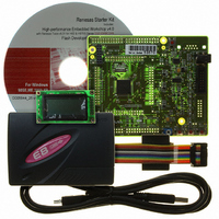
This RSK is an evaluation tool for Renesas microcontrollers. Features include: • Renesas Microcontroller Programming. • User Code Debugging. • User Circuitry such as switches, LEDs and potentiometer(s). • Sample Application. • Sample peripheral device initialisation code. The CPU board ...
Page 8
This CPU board operates from a 5V power supply. A diode provides reverse polarity protection only if a current limiting power supply is used. All CPU boards are supplied with an E8 debugger. This product is able to power ...
Page 9
Layout The following diagram shows top layer component layout of the board. LCD Display Microcontroller J3 Pin Headers Chapter 4.Board Layout Application Board Reset Switch Interface JA5 JA1 JA6 JA2 Application Board Potentiometer Interface Figure 4-1: ...
Page 10
Dimensions The following diagram gives the board dimensions and connector positions. All through hole connectors are on a common 0.1” grid for easy interfacing. Corners x4 3mm radius JA1 JA5 JA6 ...
Page 11
Chapter 5.Block Diagram Figure 5-1 shows the CPU board components and their connectivity. Application Board Headers Microcontroller Pin Headers Debug Header Option Serial Connector Option Figure 5-2 shows the connections to the RSK. Computer Power Jack Option Boot mode pins ...
Page 12
There are four switches located on the CPU board. The function of each switch and its connection are shown in Table 6-1. Switch RES When pressed; the CPU board microcontroller is reset. SW1/BOOT* Connects to an IRQ input for ...
Page 13
The microcontroller programming serial port (SCI4) is connected to the E8 connector. This serial port can optionally be connected to the RS232 transceiver by moving option resistors and fitting the D connector in position J9. The connections to ...
Page 14
Module A LCD module can be connected to the connector J13. Any module that conforms to the pin connections and has a KS0066u compatible controller can be used with the tutorial code. The LCD module uses a 4bit interface ...
Page 15
Links Table 6-6 below describes the function of the option links contained on this CPU board. The default configuration is indicated by BOLD text. Reference Function R10 Programming Serial Port R12 Programming Serial Port R15 Programming Serial Port R13 ...
Page 16
Sources A crystal oscillator is fitted on the CPU board and used to supply the main clock input to the Renesas microcontroller. Table 6-8 details the oscillators that are fitted and alternative footprints provided on this CPU board: Value ...
Page 17
The CPU board supports User mode, Boot mode and User Boot mode. User mode may be used to run and debug user code, while Boot mode may only be used to program the Renesas microcontroller with program code. User Boot ...
Page 18
The boot mode settings for this CPU board are shown in Table 7-2 below: MD1 MD0 1 0 The following picture shows these settings made in the E8Direct configuration dialog from HEW. LSI State after Reset End Boot ...
Page 19
Boot mode A Note on Mats: The H8SX/1582 possesses two distinct areas of Flash, User MAT (768KByte) and User Boot MAT (8KByte). The User Boot MAT is a separate area of FLASH from User MAT, intended to hold user ...
Page 20
Mode For the device to enter User Mode, reset must be held active while the microcontroller mode pins are held in states specified for User Mode operation. 100K pull up and pull down resistors are used to set the ...
Page 21
Chapter 8.Programming Methods All of the Flash ROM on the device (i.e. both MATs) can be programmed when the device is in Boot mode. Once in boot mode, the boot-loader program pre-programmed into the microcontroller executes and attempts a connection ...
Page 22
Headers Table 9-1 to Table 9-4 show the microcontroller pin headers and their corresponding microcontroller connections. The header pins connect directly to the microcontroller pin unless otherwise stated. Pin Circuit Net Name 1 SCIbRX 3 PIN3 5 PTTX 7 ...
Page 23
Pin Circuit Net Name 1 PIN31 3 PIN33 5 PIN35 7 PIN37 9 IO_2 11 IO_4 13 PIN43 15 IO_7 17 IRQ0 19 IRQ1 21 DLCDRS 23 IRQ3 25 SCIaRX 27 ADTRG 29 SW2 J2 Device Pin Circuit Net Name ...
Page 24
Pin Circuit Net Name 1 DLCD7 3 PIN63 5 DLCDE 7 DLCD5 9 TMR0 11 PIN71 13 PIN73 15 TMS 17 TCK 19 RESn 21 TRIGa 23 CON_XTAL 25 GROUND 27 SCIcTX 29 SCIcRX J3 Device Pin Circuit Net Name ...
Page 25
Pin Circuit Net Name 1 E8_BUSY 3 AD4 5 AD6 7 AD0 9 AD2 11 AD3 13 AD_POT 15 PIN105 17 PIN107 19 PIN109 21 PIN111 23 LED0 25 LED1 27 IIC_SCL 29 IIC_EX J4 Device Pin Circuit Net Name ...
Page 26
Headers Table 9-5 and Table 9-6 below show the standard application header connections. Pin Generic Header Name Signal Name 1 Regulated Supply Regulated Supply 2 3V3 5 Analogue Supply AVcc 7 Analogue Reference AVref 9 AD0 ...
Page 27
Pin Generic Header Name CPU board Signal Name 1 ADC4 I4 AD4 3 ADC6 I6 AD6 5 CAN CAN1TX 7 CAN CAN2TX 9 Reserved 11 Reserved 13 Reserved 15 Reserved 17 Reserved 19 Reserved 21 Reserved 23 Reserved Pin Generic ...
Page 28
Chapter 10.Code Development 10.1.Overview Note: For all code debugging using Renesas software tools, the CPU board must either be connected serial port via a serial cable USB port via an E8 ...
Page 29
Section RESET_VECTOR HMON Reset Vector (Vector 0) Required for Start-up of HMON SCI_VECTORS HMON Serial Port Vectors (Vector 160, 161, 162, 163) PHMON HMON Code CHMON HMON Constant Data BHMON HMON Un-initialised data UGenU FDT Kernel. This ...
Page 30
Map The memory map shown in this section visually describes the locations of program code sections related to HMON, the FDT kernels and the supporting code within the ROM/RAM memory areas of the microcontroller. H'0000 Vectors H'0800 CUser_Vectors H'0803 ...
Page 31
Rate Setting HMON is initially set to connect at 250000Baud. The value set in the baud rate register for the microcontroller must be altered if the user wishes to change either the serial communication baud rate of the serial ...
Page 32
Chapter 11. Component Placement 30 ...
Page 33
Chapter 12. Additional Information For details on how to use High-performance Embedded Workshop (HEW), refer to the HEW manual available on the CD or installed in the Manual Navigator. For information about the H8SX/1582 series microcontrollers refer to the H8SX/1582 ...
Page 34
REVISION HISTORY Rev. Page Date 1 25.11.2005 - Description First Release ...
Page 35
Renesas Starter Kit for H8SX1582 User's Manual Publication Date Rev.1.00 Nov 25, 2005 Published by: Renesas Technology Europe Ltd. ©2005 Renesas Technology Europe and Renesas Solutions Corp., All Rights Reserved. ...
Page 36
Renesas Starter Kit for H8SX1582 1753, Shimonumabe, Nakahara-ku, Kawasaki-shi, Kanagawa 211-8668 Japan User’s Manual REG10J0001-0100 ...