R0K561664S000BE Renesas Electronics America, R0K561664S000BE Datasheet
R0K561664S000BE
Specifications of R0K561664S000BE


Related parts for R0K561664S000BE


R0K561664S000BE Summary of contents
Page 1
To our customers, Old Company Name in Catalogs and Other Documents st On April 1 , 2010, NEC Electronics Corporation merged with Renesas Technology Corporation, and Renesas Electronics Corporation took over all the business of both companies. Therefore, although the ...
Page 2
All information included in this document is current as of the date this document is issued. Such information, however, is subject to change without any prior notice. Before purchasing or using any Renesas Electronics products listed herein, please confirm ...
Page 3
Renesas Starter Kit for H8SX1664 User’s Manual RENESAS SINGLE-CHIP MICROCOMPUTER H8SX FAMILY Rev.1.00 2006.08 ...
Page 4
Table of Contents Table of Contents ...................................................................................................................................................ii Chapter 1. Preface .................................................................................................................................................4 Chapter 2. Purpose ................................................................................................................................................5 Chapter 3. Power Supply ......................................................................................................................................6 3.1. Requirements ..............................................................................................................................................6 3.2. Power – Up Behaviour................................................................................................................................6 Chapter 4. Board Layout.......................................................................................................................................7 4.1. Component Layout......................................................................................................................................7 4.2. Board Dimensions.......................................................................................................................................8 Chapter 5. ...
Page 5
HMON Code Size ....................................................................................................................................30 10.7. Memory Map ...........................................................................................................................................32 10.8. Baud Rate Setting...................................................................................................................................33 10.9. Interrupt mask sections .........................................................................................................................33 Chapter 11. Component Placement ....................................................................................................................34 Chapter 12. Additional Information ...................................................................................................................35 iii ...
Page 6
Cautions This document may be, wholly or partially, subject to change without notice. All rights reserved. No one is permitted to reproduce or duplicate, in any form, a part or this entire document without the written permission of Renesas Technology ...
Page 7
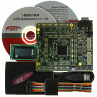
This RSK is an evaluation tool for Renesas microcontrollers. Features include: • Renesas Microcontroller Programming. • User Code Debugging. • User Circuitry such as switches, LEDs and potentiometer(s). • Sample Application. • Sample peripheral device initialisation code. The CPU board ...
Page 8
This CPU board operates from a 5V power supply. A diode provides reverse polarity protection only if a current limiting power supply is used. All CPU boards are supplied with an E8 debugger. This product is able to power ...
Page 9
Layout The following diagram shows top layer component layout of the board. LCD Display J11 USB Microcontroller J3 Pin Headers Application Interface Chapter 4.Board Layout Application Board Interface JA5 JA1 JA6 JA2 Potentiometer Board Figure 4.1: ...
Page 10
Dimensions The following diagram gives the board dimensions and connector positions. All through hole connectors are on a common 0.1” grid for easy interfacing. Figure 4.2 : Board Dimensions 8 ...
Page 11
Chapter 5.Block Diagram Figure 5.1 shows the CPU board components and their connectivity. Application Board Headers Microcontroller Pin Headers Debug Header Option USB Connector Option Serial Connector Option Figure 5.2 shows the connections to the RSK. Power Jack Option Boot ...
Page 12
There are four switches located on the CPU board. The function of each switch and its connection are shown in Table 6-1. Switch RES When pressed; the CPU board microcontroller is reset. SW1/BOOT* Connects to an IRQ input for ...
Page 13
Description Function SCI4 Tx Programming Serial Port SCI4 Rx Programming Serial Port The board is designed to accept a straight through RS232 cable. A secondary microcontroller serial port is available and connected to the application headers. Please refer to the ...
Page 14
Links Table 6-5 below describes the function of the option links contained on this CPU board. The default configuration is indicated by BOLD text. Reference Function R3 Power Source Serial Port Configuration R6 Serial Port Configuration ...
Page 15
Reference Function R34 Serial Port Configuration R35 Serial Port Configuration R36 Serial Port Configuration R37 Serial Port Configuration R40 Power Source R42 Ground Signals R44 Power Source R46 Analog Voltage Source R47 LCD Power Source R48 CON_5V Connection R49 LCD ...
Page 16
Reference Function R59 Application Board Interface R60 Application Board Interface R64 Voltage Reference Source R66 Application Board Interface R67 Application Board Interface R68 Application Board Interface R69 Up R70 Application Board Interface R71 Application Board Interface R74 Wn R75 Vp ...
Page 17
Reference Function R85 Application Board Interface R86 Wp R88 Application Board Interface R90 Application Board Interface R93 Sub Clock Oscillator Source R94 Sub Clock Oscillator Source R95 Application Board Interface R96 Application Board Interface R98 External Subclock Oscillator R99 Processor ...
Page 18
Reference Function R129 Boot Mode Selection R130 Crystal Selection R131 Memory Selection R132 Debugging Adaptor R133 Boot Mode Selection 6.7.Oscillator Sources A crystal oscillator is fitted on the CPU board and used to supply the main clock input to the ...
Page 19
Port This RSK has a Full-speed (12 Mbps) USB port compliant to USB 2.0 specification available as J12 on the RSK. This port allows Boot mode programming using USB Direct connection which does not require E8. For ...
Page 20
The CPU board supports User mode and Boot mode. User mode may be used to run and debug user code, while Boot mode may only be used to program the Renesas microcontroller with program code. To program the user boot ...
Page 21
The boot mode settings for this CPU board are shown in MD2 MD1 0 1 The following picture shows these settings made in the E8Direct configuration dialog from HEW. Table 7-2 below : MD0 LSI State after Reset ...
Page 22
User Mode For the device to enter User Mode, reset must be held active while the microcontroller mode pins are held in states specified for User Mode operation. 100K pull up and pull down resistors are used to set ...
Page 23
Chapter 8.Programming Methods All of the Flash ROM on the device (i.e. both MATs) can be programmed when the device is in Boot mode. Once in boot mode, the boot-loader program pre-programmed into the microcontroller executes and attempts a connection ...
Page 24
The Flash Development Toolkit (FDT) is supplied to allow programs to be loaded directly on to the board using this method. Please select USB Direct interface while downloading the program. 8.4.Serial Port Programming This sequence is not required when debugging ...
Page 25
Headers Table 9-1 to Table 9-4 show the microcontroller pin headers and their corresponding microcontroller connections. The header pins connect directly to the microcontroller pin unless otherwise stated. Pin Circuit Net Name 1 CS1n 3 LED0 5 DLCDD7 7 ...
Page 26
Pin Circuit Net Name EMLE 5 PM4 7 No connection 9 Ground 11 MD_CLK 13 IO0_CLK0 15 IO1_RxD0 17 IO3_UD 19 IO5_Wp 21 TIOCB0_Vn 23 IO6 25 NMIn 27 TEND1n Ground 35 ...
Page 27
Pin Circuit Net Name D10 7 Ground 9 D13 11 D15 13 IRQ1n 15 IRQ3n_ADTRG 17 CON_OSC2 19 RESn 21 TxD5 23 WDTOVF_TDO 25 CON_XTAL 27 UC_VCC 29 P1_7 31 Ground 33 TIOCA2_Up 35 PTTX ...
Page 28
Pin Circuit Net Name 1 TRSTn 3 TMS 5 TDI 7 MD0 9 LED2 11 AN1 13 CON_AVCC 15 AVss 17 CON_VREF 19 DA0_AN6 21 MD1 23 DLCDD5 25 MD3 27 WRn 29 LLWRn 31 RDn 33 Ground 35 UC_VCC ...
Page 29
Headers Table 9-5 and Table 9-6 below show the standard application header connections. Pin Generic Header Name Signal Name 1 Regulated Supply (5V) --- 3 Regulated Supply (3V3) --- 5 Analogue Supply AVcc* 7 Analogue Reference AVref* 9 AD0* ...
Page 30
Pin Generic Header Name CPU board Signal Name 1 Address Bus A0 3 Address Bus A2 5 Address Bus A4 7 Address Bus A6 9 Address Bus A8 11 Address Bus A10 13 Address Bus A12 15 Address Bus A14 ...
Page 31
Pin Generic Header Name CPU board Signal Name 1 AD4 AN4 3 AD6 AN6* 5 CAN1TX --- 7 CAN2TX --- 9 Reserved 11 Reserved 13 Reserved 15 Reserved 17 Reserved 19 Reserved 21 Reserved 23 Reserved Pin Generic Header Name ...
Page 32
Chapter 10.Code Development 10.1.Overview Note: For all code debugging using Renesas software tools, the CPU board must either be connected serial port via a serial cable USB port via an E8 ...
Page 33
Section RESET_VECTOR HMON Reset Vector (Vector 0) Required for Start-up of HMON SCI_VECTORS HMON Serial Port Vectors (Vector 160, 161, 162, 163) PHMON HMON Code CHMON HMON Constant Data BHMON HMON Un-initialised data UGenU FDT Kernel. This ...
Page 34
Map The memory map shown in this section visually describes the locations of program code sections related to HMON, the FDT kernels and the supporting code within the ROM/RAM memory areas of the microcontroller. Figure 10.1: Memory Map 32 ...
Page 35
Rate Setting HMON is initially set to connect at 250000Baud. The value set in the baud rate register for the microcontroller must be altered if the user wishes to change either the serial communication baud rate of the serial ...
Page 36
Chapter 11. Component Placement 34 ...
Page 37
Chapter 12. Additional Information For details on how to use High-performance Embedded Workshop (HEW), refer to the HEW manual available on the CD or installed in the Manual Navigator. For information about the H8SX/1664 series microcontrollers refer to the H8SX/1663 ...
Page 38
Renesas Starter Kit for H8SX1664 User's Manual Publication Date Rev.1.00 Published by: Renesas Technology Europe Ltd. Dukes Meadow, Millboard Road, Bourne End Buckinghamshire SL8 5FH, United Kingdom ©2006 Renesas Technology Europe and Renesas Solutions Corp., All Rights Reserved. ...
Page 39
Renesas Starter Kit for H8SX1664 1753, Shimonumabe, Nakahara-ku, Kawasaki-shi, Kanagawa 211-8668 Japan User’s Manual REG10J0025-0100 ...