R0K561622S000BE Renesas Electronics America, R0K561622S000BE Datasheet - Page 20
R0K561622S000BE
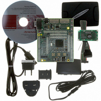
Manufacturer Part Number
R0K561622S000BE
Description
KIT STARTER FOR H8SX/1622
Manufacturer
Renesas Electronics America
Series
Renesas Starter Kits (RSK)r
Type
MCUr
Specifications of R0K561622S000BE
Contents
Board, Cables, CD, Debugger, Power Supply
Silicon Manufacturer
Renesas
Features
Coding And Debugging, E10A Emulator, RS232 Serial Connection
Kit Contents
Board
Silicon Family Name
H8SX/1622F
Silicon Core Number
R5F61622N50LGV
Lead Free Status / RoHS Status
Lead free / RoHS Compliant
For Use With/related Products
H8SX/1622
Lead Free Status / RoHS Status
Lead free / RoHS Compliant, Lead free / RoHS Compliant


12.5
12.6
12.7
12.8
12.9
12.10 Usage Notes ...................................................................................................................... 518
Section 13 Programmable Pulse Generator (PPG)............................................ 529
13.1
13.2
13.3
13.4
Rev. 2.00 Sep. 16, 2009 Page xviii of xxviii
12.4.3
12.4.4
12.4.5
12.4.6
Interrupt Sources............................................................................................................... 506
DTC Activation ................................................................................................................ 509
DMAC Activation ............................................................................................................ 509
A/D Converter Activation................................................................................................. 509
Operation Timing.............................................................................................................. 510
12.9.1
12.9.2
12.10.1 Module Stop Function Setting .......................................................................... 518
12.10.2 Input Clock Restrictions ................................................................................... 518
12.10.3 Caution on Cycle Setting .................................................................................. 519
12.10.4 Conflict between TCNT Write and Clear Operations....................................... 519
12.10.5 Conflict between TCNT Write and Increment Operations ............................... 520
12.10.6 Conflict between TGR Write and Compare Match........................................... 521
12.10.7 Conflict between Buffer Register Write and Compare Match .......................... 522
12.10.8 Conflict between TGR Read and Input Capture ............................................... 523
12.10.9 Conflict between TGR Write and Input Capture .............................................. 524
12.10.10 Conflict between Buffer Register Write and Input Capture.............................. 525
12.10.11 Conflict between Overflow/Underflow and Counter Clearing ......................... 526
12.10.12 Conflict between TCNT Write and Overflow/Underflow ................................ 527
12.10.13 Multiplexing of I/O Pins ................................................................................... 527
12.10.14 Interrupts and Module Stop State ..................................................................... 527
Features............................................................................................................................. 529
Input/Output Pins.............................................................................................................. 531
Register Descriptions........................................................................................................ 532
13.3.1
13.3.2
13.3.3
13.3.4
13.3.5
Operation .......................................................................................................................... 541
13.4.1
13.4.2
13.4.3
Buffer Operation............................................................................................... 488
Cascaded Operation .......................................................................................... 492
PWM Modes..................................................................................................... 494
Phase Counting Mode....................................................................................... 500
Input/Output Timing ......................................................................................... 510
Interrupt Signal Timing .................................................................................... 514
Next Data Enable Registers H, L (NDERH, NDERL) ..................................... 532
Output Data Registers H, L (PODRH, PODRL)............................................... 534
Next Data Registers H, L (NDRH, NDRL) ...................................................... 535
PPG Output Control Register (PCR) ................................................................ 538
PPG Output Mode Register (PMR) .................................................................. 539
Output Timing .................................................................................................. 542
Sample Setup Procedure for Normal Pulse Output........................................... 543
Example of Normal Pulse Output (Example of 5-Phase Pulse Output)............ 544
Related parts for R0K561622S000BE
Image
Part Number
Description
Manufacturer
Datasheet
Request
R

Part Number:
Description:
KIT STARTER FOR M16C/29
Manufacturer:
Renesas Electronics America
Datasheet:

Part Number:
Description:
KIT STARTER FOR R8C/2D
Manufacturer:
Renesas Electronics America
Datasheet:

Part Number:
Description:
R0K33062P STARTER KIT
Manufacturer:
Renesas Electronics America
Datasheet:

Part Number:
Description:
KIT STARTER FOR R8C/23 E8A
Manufacturer:
Renesas Electronics America
Datasheet:

Part Number:
Description:
KIT STARTER FOR R8C/25
Manufacturer:
Renesas Electronics America
Datasheet:

Part Number:
Description:
KIT STARTER H8S2456 SHARPE DSPLY
Manufacturer:
Renesas Electronics America
Datasheet:

Part Number:
Description:
KIT STARTER FOR R8C38C
Manufacturer:
Renesas Electronics America
Datasheet:

Part Number:
Description:
KIT STARTER FOR R8C35C
Manufacturer:
Renesas Electronics America
Datasheet:

Part Number:
Description:
KIT STARTER FOR R8CL3AC+LCD APPS
Manufacturer:
Renesas Electronics America
Datasheet:
Part Number:
Description:
KIT STARTER FOR RX610
Manufacturer:
Renesas Electronics America
Datasheet:

Part Number:
Description:
KIT STARTER FOR R32C/118
Manufacturer:
Renesas Electronics America
Datasheet:

Part Number:
Description:
KIT DEV RSK-R8C/26-29
Manufacturer:
Renesas Electronics America
Datasheet:

Part Number:
Description:
KIT STARTER FOR SH7124
Manufacturer:
Renesas Electronics America
Datasheet:

Part Number:
Description:
KIT DEV FOR SH7203
Manufacturer:
Renesas Electronics America
Datasheet:
Part Number:
Description:
KIT STARTER FOR R8C/18191A1B
Manufacturer:
Renesas Electronics America
Datasheet: