R0K561622S000BE Renesas Electronics America, R0K561622S000BE Datasheet - Page 25
R0K561622S000BE
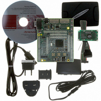
Manufacturer Part Number
R0K561622S000BE
Description
KIT STARTER FOR H8SX/1622
Manufacturer
Renesas Electronics America
Series
Renesas Starter Kits (RSK)r
Type
MCUr
Specifications of R0K561622S000BE
Contents
Board, Cables, CD, Debugger, Power Supply
Silicon Manufacturer
Renesas
Features
Coding And Debugging, E10A Emulator, RS232 Serial Connection
Kit Contents
Board
Silicon Family Name
H8SX/1622F
Silicon Core Number
R5F61622N50LGV
Lead Free Status / RoHS Status
Lead free / RoHS Compliant
For Use With/related Products
H8SX/1622
Lead Free Status / RoHS Status
Lead free / RoHS Compliant, Lead free / RoHS Compliant


18.5
18.6
18.7
Section 19 ∆Σ A/D Converter..............................................................................741
19.1
19.2
19.3
19.4
19.5
19.6
18.4.1
18.4.2
18.4.3
18.4.4
Interrupt Source ................................................................................................................ 730
A/D Conversion Accuracy Definitions ............................................................................. 730
Usage Notes ...................................................................................................................... 732
18.7.1
18.7.2
18.7.3
18.7.4
18.7.5
18.7.6
18.7.7
18.7.8
18.7.9
Features............................................................................................................................. 741
Input/Output Pins.............................................................................................................. 743
Register Descriptions........................................................................................................ 744
19.3.1
19.3.2
19.3.3
19.3.4
19.3.5
Operation .......................................................................................................................... 752
19.4.1
19.4.2
19.4.3
19.4.4
19.4.5
19.4.6
19.4.7
Interrupt Source ................................................................................................................ 766
Usage Notes ...................................................................................................................... 767
19.6.1
19.6.2
19.6.3
19.6.4
Single Mode...................................................................................................... 723
Scan Mode ........................................................................................................ 725
Input Sampling and A/D Conversion Time ...................................................... 727
External Trigger Input Timing.......................................................................... 729
Module Stop Function Setting .......................................................................... 732
A/D Input Hold Function in Software Standby Mode ...................................... 732
Notes on A/D Conversion Start by an External Trigger ................................... 732
Notes on Stopping the A/D Converter .............................................................. 734
Permissible Signal Source Impedance .............................................................. 737
Influences on Absolute Accuracy ..................................................................... 737
Setting Range of Analog Power Supply and Other Pins ................................... 738
Notes on Board Design ..................................................................................... 738
Notes on Countermeasure against Noise........................................................... 738
∆Σ A/D Mode Register (DSADMR)................................................................. 745
∆Σ A/D Data Registers 0 to 5 (DSADDR0 to DSADDR5) .............................. 746
∆Σ A/D Control/Status Register (DSADCSR).................................................. 746
∆Σ A/D Control Register (DSADCR)............................................................... 749
∆Σ A/D Offset Cancel DAC Inputs 0 to 3 (DSADOF0 to DSADOF3) ............ 751
Procedure for Activating the ∆Σ A/D Converter .............................................. 753
Selecting Analog Input Channels...................................................................... 754
Single Mode...................................................................................................... 755
Scan Mode ........................................................................................................ 758
Flow of ∆Σ A/D Conversion Operation ............................................................ 760
Analog Input Sampling and A/D Conversion Time.......................................... 762
External Trigger Input Timing.......................................................................... 765
Module Stop Function Setting .......................................................................... 767
Settings for the Biasing Circuit......................................................................... 767
State of the ∆Σ A/D Converter in Software Standby Mode .............................. 768
Changing the Settings of ∆Σ A/D Converter Registers..................................... 768
Rev. 2.00 Sep. 16, 2009 Page xxiii of xxviii
Related parts for R0K561622S000BE
Image
Part Number
Description
Manufacturer
Datasheet
Request
R

Part Number:
Description:
KIT STARTER FOR M16C/29
Manufacturer:
Renesas Electronics America
Datasheet:

Part Number:
Description:
KIT STARTER FOR R8C/2D
Manufacturer:
Renesas Electronics America
Datasheet:

Part Number:
Description:
R0K33062P STARTER KIT
Manufacturer:
Renesas Electronics America
Datasheet:

Part Number:
Description:
KIT STARTER FOR R8C/23 E8A
Manufacturer:
Renesas Electronics America
Datasheet:

Part Number:
Description:
KIT STARTER FOR R8C/25
Manufacturer:
Renesas Electronics America
Datasheet:

Part Number:
Description:
KIT STARTER H8S2456 SHARPE DSPLY
Manufacturer:
Renesas Electronics America
Datasheet:

Part Number:
Description:
KIT STARTER FOR R8C38C
Manufacturer:
Renesas Electronics America
Datasheet:

Part Number:
Description:
KIT STARTER FOR R8C35C
Manufacturer:
Renesas Electronics America
Datasheet:

Part Number:
Description:
KIT STARTER FOR R8CL3AC+LCD APPS
Manufacturer:
Renesas Electronics America
Datasheet:
Part Number:
Description:
KIT STARTER FOR RX610
Manufacturer:
Renesas Electronics America
Datasheet:

Part Number:
Description:
KIT STARTER FOR R32C/118
Manufacturer:
Renesas Electronics America
Datasheet:

Part Number:
Description:
KIT DEV RSK-R8C/26-29
Manufacturer:
Renesas Electronics America
Datasheet:

Part Number:
Description:
KIT STARTER FOR SH7124
Manufacturer:
Renesas Electronics America
Datasheet:

Part Number:
Description:
KIT DEV FOR SH7203
Manufacturer:
Renesas Electronics America
Datasheet:
Part Number:
Description:
KIT STARTER FOR R8C/18191A1B
Manufacturer:
Renesas Electronics America
Datasheet: