R0K561622S000BE Renesas Electronics America, R0K561622S000BE Datasheet - Page 316
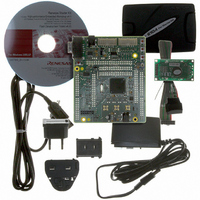
R0K561622S000BE
Manufacturer Part Number
R0K561622S000BE
Description
KIT STARTER FOR H8SX/1622
Manufacturer
Renesas Electronics America
Series
Renesas Starter Kits (RSK)r
Type
MCUr
Specifications of R0K561622S000BE
Contents
Board, Cables, CD, Debugger, Power Supply
Silicon Manufacturer
Renesas
Features
Coding And Debugging, E10A Emulator, RS232 Serial Connection
Kit Contents
Board
Silicon Family Name
H8SX/1622F
Silicon Core Number
R5F61622N50LGV
Lead Free Status / RoHS Status
Lead free / RoHS Compliant
For Use With/related Products
H8SX/1622
Lead Free Status / RoHS Status
Lead free / RoHS Compliant, Lead free / RoHS Compliant


Section 9 DMA Controller (DMAC)
9.5
9.5.1
(1)
In dual address mode, the transfer source address is specified in DSAR and the transfer destination
address is specified in DDAR. A transfer at a time is performed in two bus cycles (when the data
bus width is less than the data access size or the access address is not aligned with the boundary of
the data access size, the number of bus cycles are needed more than two because one bus cycle is
divided into multiple bus cycles).
In the first bus cycle, data at the transfer source address is read and in the next cycle, the read data
is written to the transfer destination address.
The read and write cycles are not separated. Other bus cycles (bus cycle by other bus masters,
refresh cycle, and external bus release cycle) are not generated between read and write cycles.
The TEND signal output is enabled or disabled by the TENDE bit in DMDR. The TEND signal is
output in two bus cycles. When an idle cycle is inserted before the bus cycle, the TEND signal is
also output in the idle cycle. The DACK signal is not output.
Figure 9.2 shows an example of the signal timing in dual address mode and figure 9.3 shows the
operation in dual address mode.
Rev. 2.00 Sep. 16, 2009 Page 286 of 1036
REJ09B0414-0200
Dual Address Mode
Operations
Address Modes
Figure 9.2 Example of Signal Timing in Dual Address Mode
Bφ
Address bus
RD
WR
TEND
DMA read
cycle
DSAR
DMA write
DDAR
cycle
Related parts for R0K561622S000BE
Image
Part Number
Description
Manufacturer
Datasheet
Request
R

Part Number:
Description:
KIT STARTER FOR M16C/29
Manufacturer:
Renesas Electronics America
Datasheet:

Part Number:
Description:
KIT STARTER FOR R8C/2D
Manufacturer:
Renesas Electronics America
Datasheet:

Part Number:
Description:
R0K33062P STARTER KIT
Manufacturer:
Renesas Electronics America
Datasheet:

Part Number:
Description:
KIT STARTER FOR R8C/23 E8A
Manufacturer:
Renesas Electronics America
Datasheet:

Part Number:
Description:
KIT STARTER FOR R8C/25
Manufacturer:
Renesas Electronics America
Datasheet:

Part Number:
Description:
KIT STARTER H8S2456 SHARPE DSPLY
Manufacturer:
Renesas Electronics America
Datasheet:

Part Number:
Description:
KIT STARTER FOR R8C38C
Manufacturer:
Renesas Electronics America
Datasheet:

Part Number:
Description:
KIT STARTER FOR R8C35C
Manufacturer:
Renesas Electronics America
Datasheet:

Part Number:
Description:
KIT STARTER FOR R8CL3AC+LCD APPS
Manufacturer:
Renesas Electronics America
Datasheet:
Part Number:
Description:
KIT STARTER FOR RX610
Manufacturer:
Renesas Electronics America
Datasheet:

Part Number:
Description:
KIT STARTER FOR R32C/118
Manufacturer:
Renesas Electronics America
Datasheet:

Part Number:
Description:
KIT DEV RSK-R8C/26-29
Manufacturer:
Renesas Electronics America
Datasheet:

Part Number:
Description:
KIT STARTER FOR SH7124
Manufacturer:
Renesas Electronics America
Datasheet:

Part Number:
Description:
KIT DEV FOR SH7203
Manufacturer:
Renesas Electronics America
Datasheet:
Part Number:
Description:
KIT STARTER FOR R8C/18191A1B
Manufacturer:
Renesas Electronics America
Datasheet: