R0K561622S000BE Renesas Electronics America, R0K561622S000BE Datasheet - Page 792
R0K561622S000BE
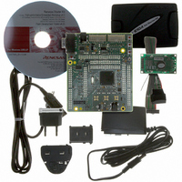
Manufacturer Part Number
R0K561622S000BE
Description
KIT STARTER FOR H8SX/1622
Manufacturer
Renesas Electronics America
Series
Renesas Starter Kits (RSK)r
Type
MCUr
Specifications of R0K561622S000BE
Contents
Board, Cables, CD, Debugger, Power Supply
Silicon Manufacturer
Renesas
Features
Coding And Debugging, E10A Emulator, RS232 Serial Connection
Kit Contents
Board
Silicon Family Name
H8SX/1622F
Silicon Core Number
R5F61622N50LGV
Lead Free Status / RoHS Status
Lead free / RoHS Compliant
For Use With/related Products
H8SX/1622
Lead Free Status / RoHS Status
Lead free / RoHS Compliant, Lead free / RoHS Compliant


Section 19 ∆Σ A/D Converter
19.4.6
After the ADST bit in DSADCSR has been set to 1 to initiate conversion, the ∆Σ A/D converter
only starts sampling the analog inputs after the ∆Σ A/D converter start-up delay time (t
to wait for the ∆Σ modulator to be stabilized (t
analog input and converts it to a sequence of digital values, which is then passed through a digital
filter. The A/D conversion ends after the input sampling time (t
modulator stop delay time (t
Figure 19.8 shows the timing of A/D conversion, and tables 19.5 and 19.6 show A/D conversion
times. As shown in figure 19.8, the A/D conversion time is a total of four periods. t
vary because they are determined by the timing of synchronization between different clock signals
and the state of control of synchronization processing at the end of the previous round of A/D
conversion. For this reason, conversion times vary within the range shown in table 19.5.
Rev. 2.00 Sep. 16, 2009 Page 762 of 1036
REJ09B0414-0200
(1)
(2)
t
t
t
t
[Legend]
t
SD
SWT
SPLT
CONV
ED
internal reset signal
∆Σ modulator
Write signal
Input sampling
timing signal
Address
: DSADCSR write cycle
: Address of DSADCSR
: ∆Σ A/D converter start delay time
: ∆Σ modulator stabilization wait time
: Input sampling time
: ∆Σ A/D converter stop delay time
: A/D conversion time (first conversion)
Analog Input Sampling and A/D Conversion Time
ADST
Figure 19.8 A/D Conversion Timing (Single Mode, Once, One Channel)
ADF
(1)
(2)
t
ED
SD
) have elapsed.
t
SWT
SWT
) have elapsed. The ∆Σ modulator samples the
t
CONV
t
SPLT
SPLT
) and the subsequent ∆Σ
t
ED
SD
and t
SD
) and time
ED
can
Related parts for R0K561622S000BE
Image
Part Number
Description
Manufacturer
Datasheet
Request
R

Part Number:
Description:
KIT STARTER FOR M16C/29
Manufacturer:
Renesas Electronics America
Datasheet:

Part Number:
Description:
KIT STARTER FOR R8C/2D
Manufacturer:
Renesas Electronics America
Datasheet:

Part Number:
Description:
R0K33062P STARTER KIT
Manufacturer:
Renesas Electronics America
Datasheet:

Part Number:
Description:
KIT STARTER FOR R8C/23 E8A
Manufacturer:
Renesas Electronics America
Datasheet:

Part Number:
Description:
KIT STARTER FOR R8C/25
Manufacturer:
Renesas Electronics America
Datasheet:

Part Number:
Description:
KIT STARTER H8S2456 SHARPE DSPLY
Manufacturer:
Renesas Electronics America
Datasheet:

Part Number:
Description:
KIT STARTER FOR R8C38C
Manufacturer:
Renesas Electronics America
Datasheet:

Part Number:
Description:
KIT STARTER FOR R8C35C
Manufacturer:
Renesas Electronics America
Datasheet:

Part Number:
Description:
KIT STARTER FOR R8CL3AC+LCD APPS
Manufacturer:
Renesas Electronics America
Datasheet:
Part Number:
Description:
KIT STARTER FOR RX610
Manufacturer:
Renesas Electronics America
Datasheet:

Part Number:
Description:
KIT STARTER FOR R32C/118
Manufacturer:
Renesas Electronics America
Datasheet:

Part Number:
Description:
KIT DEV RSK-R8C/26-29
Manufacturer:
Renesas Electronics America
Datasheet:

Part Number:
Description:
KIT STARTER FOR SH7124
Manufacturer:
Renesas Electronics America
Datasheet:

Part Number:
Description:
KIT DEV FOR SH7203
Manufacturer:
Renesas Electronics America
Datasheet:
Part Number:
Description:
KIT STARTER FOR R8C/18191A1B
Manufacturer:
Renesas Electronics America
Datasheet: