MPC8349E-MITXE Freescale Semiconductor, MPC8349E-MITXE Datasheet - Page 10
MPC8349E-MITXE
Manufacturer Part Number
MPC8349E-MITXE
Description
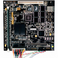
BOARD REFERENCE FOR MPC8349
Manufacturer
Freescale Semiconductor
Series
PowerQUICC II™ PROr
Type
MPUr
Specifications of MPC8349E-MITXE
Contents
Module and Misc Hardware
Processor To Be Evaluated
MPC8349E
Interface Type
Ethernet, USB
Silicon Manufacturer
Freescale
Core Architecture
Power Architecture
Core Sub-architecture
PowerQUICC
Silicon Core Number
MPC83xx
Silicon Family Name
PowerQUICC II PRO
Rohs Compliant
Yes
For Use With/related Products
MPC8349E
Lead Free Status / RoHS Status
Lead free / RoHS Compliant
Other names
MPC8349E-MITXE


MPC8349E-mITXE Board
A boot Flash selector jumper allows the user to select between two different boot images in each bank of
Flash memory.
1.2.7
The MPC8349E has two I
master for both I
is connected to the DDR DIMM module SPD (serial presence detect) EEPROM, the two PCF8574 I
expanders, the DS1339 RTC (real time clock) and the I
The M24256 serial EEPROM can be used to store the reset configuration word of the MPC8349E, as well
as storing the configuration registers values if boot sequencer of MPC8349E is enabled. If user wants to
load the reset configuration word from the I2C1 M24256 EEPROM, the jumper J22 should be set to
ABCDEFGH=01011110, with 1=jumper removed and 0=jumper installed. For more details on how to
program the reset configuration word value in I
the MPC8349ERM. The I
The DDR SPD EEPROM is connected to the I2C2 of MPC8349E. The bootload program optionally reads
the SPD EEPROM data to determine the DDR DIMM physical structure (e.g. number of rows and
columns), the DDR timings (e.g. CAS latency, re-fresh timing), and setup the configuration registers of
the MPC8349E DDR memory controller. The I
There are two PCF8574A I
I/O expansion via the I2C2 interface. The first PCF8574A (U8) has I2C2 address 0x38 and it is able to
control the Green LED (D1) and Yellow LED (D2), set the VSC8201 to powerdown mode, set the logic
level of PCI_PME signal of the miniPCI card, and enable the LCD interface of the MPC8349E-mITXE
board. The bit definition of this PCF8574A (U8) is defined as in
10
I
2
C
2
Jumper Off
Jumper On
C buses (I2C1 and I2C2). I2C1 is connected to the M24256 serial EEPROM, and I2C2
J22.E
Backup Flash
Boot Flash
MPC8349E-mITXE Reference Design Platform User’s Guide, Rev. 2
2
2
C address of the M24256 EEPROM on I2C1 bus is 0x50.
C interfaces. On the MPC8349E-mITXE board, the MPC8349E acts as I
2
C I/O expander on the MPC8349E-mITXE board to provide general purpose
BOOT1
Preliminary—Subject to Change Without Notice
1
0
Table 2. Boot Flash Selection
Table 3. Flash Memory Map
2
2
C address of the DDR SPD EEPROM on I2C2 bus is 0x51.
0xFE80_0000 to 0xFEFF_FFFF
0xFE00_0000 to 0xFE7F_FFFF
C EEPROM and the boot sequencer mode, please refer to
Boot Flash
16 Mbyte MX29LV640M
U4
U7
2
(2 × 8 Mbyte)
C interface of the MC9S08QG8.
Table
4.
Backup Flash
U7
U4
Freescale Semiconductor
2
2
C
C
Related parts for MPC8349E-MITXE
Image
Part Number
Description
Manufacturer
Datasheet
Request
R

Part Number:
Description:
KIT REFERENCE PLATFORM MPC8349E
Manufacturer:
Freescale Semiconductor
Datasheet:
Part Number:
Description:
KIT MODULAR DEV SYSTEM MPC8349E
Manufacturer:
Freescale Semiconductor
Datasheet:

Part Number:
Description:
MCU, MPU & DSP Development Tools PROCESSR BD MPC8349E
Manufacturer:
Freescale Semiconductor
Part Number:
Description:
MCU, MPU & DSP Development Tools KIT FOR MPC8349E BDS
Manufacturer:
Freescale Semiconductor

Part Number:
Description:
Manufacturer:
Freescale Semiconductor, Inc
Datasheet:
Part Number:
Description:
Manufacturer:
Freescale Semiconductor, Inc
Datasheet:
Part Number:
Description:
Manufacturer:
Freescale Semiconductor, Inc
Datasheet:
Part Number:
Description:
Manufacturer:
Freescale Semiconductor, Inc
Datasheet:
Part Number:
Description:
Manufacturer:
Freescale Semiconductor, Inc
Datasheet:
Part Number:
Description:
Manufacturer:
Freescale Semiconductor, Inc
Datasheet:
Part Number:
Description:
Manufacturer:
Freescale Semiconductor, Inc
Datasheet:
Part Number:
Description:
Manufacturer:
Freescale Semiconductor, Inc
Datasheet:
Part Number:
Description:
Manufacturer:
Freescale Semiconductor, Inc
Datasheet:
Part Number:
Description:
Manufacturer:
Freescale Semiconductor, Inc
Datasheet:
Part Number:
Description:
Manufacturer:
Freescale Semiconductor, Inc
Datasheet: