DK-DEV-4SE530N Altera, DK-DEV-4SE530N Datasheet
DK-DEV-4SE530N
Specifications of DK-DEV-4SE530N
Available stocks


Related parts for DK-DEV-4SE530N


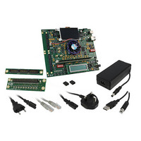
DK-DEV-4SE530N Summary of contents
Page 1
... Innovation Drive San Jose, CA 95134 www.altera.com UG-01067-2.0 Stratix IV E FPGA Development Kit User Guide ...
Page 2
... U.S. and foreign patents and pending applications, maskwork rights, and copyrights. Altera warrants performance of its semiconductor products to current specifications in accordance with Altera's standard warranty, but reserves the right to make changes to any products and services at any time without notice. Altera assumes no responsibility or liability arising out of the application or use of any information, product, or service described herein except as expressly agreed to in writing by Altera ...
Page 3
... Connecting to the Board Update Portal Web Page . . . . . . . . . . . . . . . . . . . . . . . . . . . . . . . . . . . . . . . . . . . 5–1 Using the Board Update Portal to Update User Designs . . . . . . . . . . . . . . . . . . . . . . . . . . . . . . . . . . . . . . 5–2 Chapter 6. Board Test System Introduction . . . . . . . . . . . . . . . . . . . . . . . . . . . . . . . . . . . . . . . . . . . . . . . . . . . . . . . . . . . . . . . . . . . . . . . . . . . . 6–1 Preparing the Board . . . . . . . . . . . . . . . . . . . . . . . . . . . . . . . . . . . . . . . . . . . . . . . . . . . . . . . . . . . . . . . . . . . . . 6–3 Running the Board Test System . . . . . . . . . . . . . . . . . . . . . . . . . . . . . . . . . . . . . . . . . . . . . . . . . . . . . . . . . . . 6–3 © May 2010 Altera Corporation Contents Stratix IV E FPGA Development Kit User Guide ...
Page 4
... Number of Addresses to Write and Read . . . . . . . . . . . . . . . . . . . . . . . . . . . . . . . . . . . . . . . . . . . . . 6–15 Data Type . . . . . . . . . . . . . . . . . . . . . . . . . . . . . . . . . . . . . . . . . . . . . . . . . . . . . . . . . . . . . . . . . . . . . . . . 6–15 Read and Write Control . . . . . . . . . . . . . . . . . . . . . . . . . . . . . . . . . . . . . . . . . . . . . . . . . . . . . . . . . . . . 6–15 The HSMC Tab . . . . . . . . . . . . . . . . . . . . . . . . . . . . . . . . . . . . . . . . . . . . . . . . . . . . . . . . . . . . . . . . . . . . . . 6–15 Status . . . . . . . . . . . . . . . . . . . . . . . . . . . . . . . . . . . . . . . . . . . . . . . . . . . . . . . . . . . . . . . . . . . . . . . . . . . . 6–16 Data Type . . . . . . . . . . . . . . . . . . . . . . . . . . . . . . . . . . . . . . . . . . . . . . . . . . . . . . . . . . . . . . . . . . . . . . . . 6–17 Error Control . . . . . . . . . . . . . . . . . . . . . . . . . . . . . . . . . . . . . . . . . . . . . . . . . . . . . . . . . . . . . . . . . . . . . 6–17 Start . . . . . . . . . . . . . . . . . . . . . . . . . . . . . . . . . . . . . . . . . . . . . . . . . . . . . . . . . . . . . . . . . . . . . . . . . . . . . 6–17 Stop . . . . . . . . . . . . . . . . . . . . . . . . . . . . . . . . . . . . . . . . . . . . . . . . . . . . . . . . . . . . . . . . . . . . . . . . . . . . . 6–17 Performance Indicators . . . . . . . . . . . . . . . . . . . . . . . . . . . . . . . . . . . . . . . . . . . . . . . . . . . . . . . . . . . . . 6–17 Stratix IV E FPGA Development Kit User Guide © May 2010 Altera Corporation ...
Page 5
... Restoring the Flash Device to the Factory Settings . . . . . . . . . . . . . . . . . . . . . . . . . . . . . . . . . . . . . . . . . . A–4 Restoring the MAX II CPLD to the Factory Settings . . . . . . . . . . . . . . . . . . . . . . . . . . . . . . . . . . . . . . . . . A–5 Additional Information Revision History . . . . . . . . . . . . . . . . . . . . . . . . . . . . . . . . . . . . . . . . . . . . . . . . . . . . . . . . . . . . . . . . . . . . . Info–1 How to Contact Altera . . . . . . . . . . . . . . . . . . . . . . . . . . . . . . . . . . . . . . . . . . . . . . . . . . . . . . . . . . . . . . . . Info–1 Typographic Conventions . . . . . . . . . . . . . . . . . . . . . . . . . . . . . . . . . . . . . . . . . . . . . . . . . . . . . . . . . . . . . Info–1 © May 2010 Altera Corporation v Stratix IV E FPGA Development Kit User Guide ...
Page 6
... Stratix IV E FPGA Development Kit User Guide © May 2010 Altera Corporation ...
Page 7
... Take advantage of the modular and scalable design by using the high-speed mezzanine card (HSMC) connectors to interface to over 20 different HSMCs provided by Altera partners, supporting protocols such as Serial RapidIO 10 Gigabit Ethernet, SONET, Common Public Radio Interface (CPRI), Open Base Station Architecture Initiative (OBSAI) and others ■ ...
Page 8
... EDA tools. f The kit includes a development kit edition (DKE) license for the Quartus II software (Windows platform only). This license entitles you to all the features of the subscription edition for a period of one year. After the year, you must purchase a renewal subscription to continue using the software ...
Page 9
... Download the Stratix IV E FPGA Development Kit installer from the FPGA Development Kit development kit DVD from the the Altera website. © May 2010 Altera Corporation page of the Altera website. Alternatively, you can request a Altera Kit Installations DVD Request Form Stratix IV E FPGA Development Kit User Guide 1–3 Stratix IV E ...
Page 10
... Stratix IV E FPGA Development Kit User Guide Chapter 1: About This Kit Kit Features © May 2010 Altera Corporation ...
Page 11
... For more information about power consumption and thermal modeling, refer to AN 358: Thermal Management for References Use the following links to check the Altera website for other related information: © May 2010 Altera Corporation 2. Getting Started Manual. “Kit Features” on page FPGAs ...
Page 12
... For Nios II 32-bit embedded processor solutions, refer to the ■ Processing Stratix IV E FPGA Development Kit User Guide page. page. page. Chapter 2: Getting Started References Stratix IV E Development Literature: Stratix IV Devices page. Capture CIS Symbols page. Embedded © May 2010 Altera Corporation ...
Page 13
... Licensing for Windows and Linux Licensing Considerations Purchasing this kit entitles you to a one-year DKE license for the Quartus II Subscription Edition Software. Before using the Quartus II software, you must obtain and install a license file. If you already have a licensed version of the subscription edition, you can use that license file with this kit ...
Page 14
... Follow the on-screen instructions to request your license. Altera sends you a license file through email install your license, refer to Specifying the License File in Licensing for Windows and Linux Installing the Stratix IV E FPGA Development Kit To install the Stratix IV E FPGA Development Kit, perform the following steps: 1 ...
Page 15
... Installation instructions for the USB-Blaster driver for your operating system are available on the Altera website. On the page of the Altera website, locate the table entry for your configuration and click the link to access the instructions. © May 2010 Altera Corporation Altera Programming Cable Driver Information Stratix IV E FPGA Development Kit User Guide 3– ...
Page 16
... Stratix IV E FPGA Development Kit User Guide Chapter 3: Software Installation Installing the USB-Blaster Driver © May 2010 Altera Corporation ...
Page 17
... Stratix IV E device configured successfully. f For more information about the PFL megafunction, refer to Flash Loader with the Quartus II © May 2010 Altera Corporation 4. Development Board Setup shows the switch location on the Stratix IV E FPGA development Software. to return the board to its factory ...
Page 18
... SHUNT = 1.8V_QDR J21 SW4 OPEN VCC_VCCL_SEL Board Settings Chapter 4: Development Board Setup Factory Default Switch Settings SW1 J2 J4 MSEL0 Clock USB Enable J10 SW2 OPEN MAX II DIPSWITCH J18 SHUNT = 1.8V_RLD SW5 Rotary Switch 0 PGM CONFIG SELECT © May 2010 Altera Corporation ...
Page 19
... When off, the 100 Mhz clock is enabled. ■ 4 CLK125_EN Switch 4 has the following options: When on, the 125 Mhz clock is disabled ■ When off, the 125 Mhz clock is enabled ■ © May 2010 Altera Corporation J28 50 60 MAX RLD_ZQ_IMPED J29 Table 4–1 Function 4– ...
Page 20
... Stratix IV E FPGA Development Kit User Guide Chapter 4: Development Board Setup Factory Default Switch Settings Table 4–2 and Figure 4–2. Function Table 4–3 and Figure 4–1. Function © May 2010 Altera Corporation Default Position Closed Closed Closed Closed Closed Closed Closed Closed Default Position ...
Page 21
... The HSMC port B JTAG enable jumper has the following options: Installing the shunt includes HSMC port B in the JTAG chain. ■ Removing the shunt removes HSMC port B from the JTAG chain. ■ © May 2010 Altera Corporation Function Table 4–4, Figure 4– ...
Page 22
... Stratix IV E FPGA Development Kit User Guide Chapter 4: Development Board Setup Function Manual. Factory Default Switch Settings Default Shunt Position Installed on pins 3 and 4 Installed Not installed Not installed Not installed Installed on pins 1 and 2 Not installed Stratix IV E FPGA © May 2010 Altera Corporation ...
Page 23
... Chapter 4: Development Board Setup Factory Default Switch Settings © May 2010 Altera Corporation 4–7 Stratix IV E FPGA Development Kit User Guide ...
Page 24
... Stratix IV E FPGA Development Kit User Guide Chapter 4: Development Board Setup Factory Default Switch Settings © May 2010 Altera Corporation ...
Page 25
... The web page allows you to upload new FPGA designs to the user hardware portion of flash memory, and provides links to useful information on the Altera website, including links to kit-specific and design resources. ...
Page 26
... Board Update Portal web page the Hardware File Name field specify the .flash file that you either downloaded from the Altera website or created on your own. If there is a software component to the design, specify it in the same manner using the Software File Name field, otherwise leave the Software File Name field blank ...
Page 27
... A GUI runs on the PC which communicates over the JTAG bus to a test design running in the Stratix IV E device. in the factory configuration. © May 2010 Altera Corporation 6. Board Test System 3–2. Figure 6–1 shows the initial GUI for a board that is ...
Page 28
... JTAG bus, other applications using the JTAG bus might time out. Be sure to close the other applications before attempting to reconfigure the FPGA using the Quartus II Programmer. Stratix IV E FPGA Development Kit User Guide Chapter 6: Board Test System Introduction ® II Embedded Logic © May 2010 Altera Corporation ...
Page 29
... BoardTestSystem.exe application Windows, click Start > All Programs > Altera > Stratix IV E FPGA Development Kit <version> > Board Test System to run the application. A GUI appears, displaying the application tab that corresponds to the design running in the FPGA. The Stratix IV E FPGA development board’s flash memory ships preconfigured with the design that corresponds to the Config, GPIO, and SRAM& ...
Page 30
... The Board information controls display static information about your board. ■ ■ Stratix IV E FPGA Development Kit User Guide shows the Config tab. The tab displays the contents of the Chapter 6: Board Test System Using the Board Test System © May 2010 Altera Corporation ...
Page 31
... JTAG Chain The JTAG chain control shows all the devices currently in the JTAG chain. The Stratix IV E device is always the first device in the chain. © May 2010 Altera Corporation Stratix IV E FPGA Development Kit Table 6–1. Changes to the register values with the GUI ...
Page 32
... Figure 6–3 Figure 6–3. The GPIO Tab The following sections describe the controls on the GPIO tab. Stratix IV E FPGA Development Kit User Guide shows the GPIO tab. Chapter 6: Board Test System Using the Board Test System © May 2010 Altera Corporation ...
Page 33
... FPGA during configuration. The SRAM&Flash Tab The SRAM&Flash tab allows you to read and write SRAM and flash memory on your board. Figure 6–4 © May 2010 Altera Corporation shows the SRAM&Flash tab. 6–7 Stratix IV E FPGA Development Kit User Guide ...
Page 34
... SRAM and then reads the values back to guarantee that the graphical display accurately reflects the memory contents. Stratix IV E FPGA Development Kit User Guide Chapter 6: Board Test System Using the Board Test System © May 2010 Altera Corporation ...
Page 35
... The DDR3 Tab The DDR3 tab allows you to read and write the DDR3 memory on your board. Figure 6–5 shows the DDR3 tab. © May 2010 Altera Corporation Table A–1 on page A–1). 6–9 Figure 6–1 on Stratix IV E FPGA Development Kit User Guide ...
Page 36
... Write, Read, and Total performance bars—Show the percentage of maximum theoretical data rate that the requested transactions are able to achieve. Stratix IV E FPGA Development Kit User Guide Chapter 6: Board Test System Using the Board Test System © May 2010 Altera Corporation ...
Page 37
... Write only—Selects write transactions for analysis. The QDRII+ Tab The QDRII+ tab allows you to read and write the QDR II+ memory on your board. Figure 6–6 shows the QDRII+ tab. © May 2010 Altera Corporation 6–11 Stratix IV E FPGA Development Kit User Guide ...
Page 38
... Write and Read performance bars—Show the percentage of maximum theoretical data rate that the requested transactions are able to achieve. Stratix IV E FPGA Development Kit User Guide Chapter 6: Board Test System Using the Board Test System © May 2010 Altera Corporation ...
Page 39
... Math—Selects data generated from a simple math function within the FPGA fabric. The RLDRAMII Tab The RLDRAMII tab allows you to read and write the RLDRAM II on your board. Figure 6–5 shows the RLDRAMII tab. © May 2010 Altera Corporation 6–13 Stratix IV E FPGA Development Kit User Guide ...
Page 40
... Write, Read, and Total performance bars—Show the percentage of maximum theoretical data rate that the requested transactions are able to achieve. Stratix IV E FPGA Development Kit User Guide Chapter 6: Board Test System Using the Board Test System © May 2010 Altera Corporation ...
Page 41
... Write only—Selects write transactions for analysis. The HSMC Tab The HSMC tab allows you to perform loopback tests on the HSMC A and HSMC B ports. Figure 6–8 © May 2010 Altera Corporation shows the HSMC tab. 6–15 Stratix IV E FPGA Development Kit User Guide ...
Page 42
... The Port control allows you to specify the type of test to run on the HSMC ports. The following HSMC port tests are available: Stratix IV E FPGA Development Kit User Guide Chapter 6: Board Test System Using the Board Test System © May 2010 Altera Corporation ...
Page 43
... SERDES port. The x3 single-ended data bus is 3 bits wide and clocked using a 100 MHz clock single-data-rate for 100 Mbps per pin 300 Mbps bandwidth for each x3 single-ended data port. © May 2010 Altera Corporation 6–17 Stratix IV E FPGA Development Kit User Guide ...
Page 44
... You can also run the Power Monitor as a stand-alone application. PowerTool.exe resides in the <install dir>\kits\stratixIVE_4se530_fpga\examples\board_test_system directory. On Windows, click Start > All Programs > Altera > Stratix IV E FPGA Development Kit <version> > Power Monitor to start the application. The Power Monitor communicates with the MAX II device on the board through the JTAG bus ...
Page 45
... The yellow line indicates the minimum value read since the last reset. Graph Settings The following Graph settings controls allow you to define the look and feel of the power graph: © May 2010 Altera Corporation Stratix IV E FPGA Development Kit Stratix IV E Manual. Stratix IV E FPGA Development Kit User Guide 6– ...
Page 46
... JTAG-based applications such as the Board Test System and the Power Monitor to loose their connection to the board. Restart those applications after configuration is complete. Stratix IV E FPGA Development Kit User Guide Chapter 6: Board Test System Configuring the FPGA Using the Quartus II Programmer © May 2010 Altera Corporation ...
Page 47
... Introduction As you develop your own project using the Altera tools, you can program the flash memory device so that your own design loads from flash memory into the FPGA on power up. This appendix describes the preprogrammed contents of the common flash interface (CFI) flash memory device on the Stratix IV E FPGA development board and the Nios II EDS tools involved with reprogramming the user portions of the flash memory device ...
Page 48
... If you have an FPGA design developed using the Quartus II software, and software developed using the Nios II EDS, follow these instructions the Windows Start menu, click All Programs > Altera > Nios II EDS > Nios II Command Shell the Nios II command shell, navigate to the directory where your design files reside and type the following Nios II EDS commands: For Quartus II ...
Page 49
... The CONF DONE LED (D22) and the eight user LEDs (D23-D30) illuminate indicating that the flash device is ready for programming the Windows Start menu, click All Programs > Altera > Nios II EDS > Nios II Command Shell the Nios II command shell, navigate to the <install dir> ...
Page 50
... The CONF DONE LED (D22) and the eight user LEDs (D23-D30) illuminate indicating that the flash device is ready for programming the Windows Start menu, click All Programs > Altera > Nios II EDS > Nios II Command Shell the Nios II command shell, navigate to the <install dir> ...
Page 51
... To ensure that you have the most up-to-date factory restore files and information about this product, refer to the website. © May 2010 Altera Corporation Stratix IV E FPGA Development Kit 4–2. Stratix IV E FPGA Development Kit Stratix IV E FPGA Development Kit User Guide A– ...
Page 52
... A–6 Stratix IV E FPGA Development Kit User Guide Appendix A: Programming the Flash Memory Device Restoring the MAX II CPLD to the Factory Settings © May 2010 Altera Corporation ...
Page 53
... Product literature Non-technical support (General) Email (Software Licensing) Email Note to Table: (1) You can also contact your local Altera sales office or sales representative. Typographic Conventions This document uses the typographic conventions shown in the following table. Visual Cue Bold Type with Initial Capital ...
Page 54
... A warning calls attention to a condition or possible situation that can cause you injury. The angled arrow instructs you to press Enter. The feet direct you to more information about a particular topic. Additional Information Typographic Conventions © May 2010 Altera Corporation ...