DK-DEV-2AGX260N Altera, DK-DEV-2AGX260N Datasheet
DK-DEV-2AGX260N
Specifications of DK-DEV-2AGX260N
Available stocks


Related parts for DK-DEV-2AGX260N


DK-DEV-2AGX260N Summary of contents
Page 1
... Arria II GX FPGA Development Kit, 6G Edition User Guide Arria II GX FPGA Development Kit, 6G Edition 101 Innovation Drive San Jose, CA 95134 www.altera.com UG-01084-1.0 User Guide Subscribe ...
Page 2
... Altera warrants performance of its semiconductor products to current specifications in accordance with Altera's standard warranty, but reserves the right to make changes to any products and services at any time without notice. Altera assumes no responsibility or liability arising out of the application or use of any information, product, or service described herein except as expressly agreed to in writing by Altera. Altera customers are advised to obtain the latest version of device specifications before relying on any published information and before placing orders for products or services ...
Page 3
... JTAG Chain Devices . . . . . . . . . . . . . . . . . . . . . . . . . . . . . . . . . . . . . . . . . . . . . . . . . . . . . . . . . . . . . . . . 6–6 Flash Memory Map . . . . . . . . . . . . . . . . . . . . . . . . . . . . . . . . . . . . . . . . . . . . . . . . . . . . . . . . . . . . . . . . . 6–6 The GPIO Tab . . . . . . . . . . . . . . . . . . . . . . . . . . . . . . . . . . . . . . . . . . . . . . . . . . . . . . . . . . . . . . . . . . . . . . . . 6–7 Character LCD . . . . . . . . . . . . . . . . . . . . . . . . . . . . . . . . . . . . . . . . . . . . . . . . . . . . . . . . . . . . . . . . . . . . . 6–7 User DIP Switches . . . . . . . . . . . . . . . . . . . . . . . . . . . . . . . . . . . . . . . . . . . . . . . . . . . . . . . . . . . . . . . . . . 6–7 User LEDs . . . . . . . . . . . . . . . . . . . . . . . . . . . . . . . . . . . . . . . . . . . . . . . . . . . . . . . . . . . . . . . . . . . . . . . . . 6–8 Push Button Switches . . . . . . . . . . . . . . . . . . . . . . . . . . . . . . . . . . . . . . . . . . . . . . . . . . . . . . . . . . . . . . . 6–8 The SRAM&Flash Tab . . . . . . . . . . . . . . . . . . . . . . . . . . . . . . . . . . . . . . . . . . . . . . . . . . . . . . . . . . . . . . . . . 6–8 July 2010 Altera Corporation Contents Arria II GX FPGA Development Kit, 6G Edition User Guide ...
Page 4
... Restoring the Flash Device to the Factory Settings . . . . . . . . . . . . . . . . . . . . . . . . . . . . . . . . . . . . . . . . . . A–4 Restoring the MAX II CPLD to the Factory Settings . . . . . . . . . . . . . . . . . . . . . . . . . . . . . . . . . . . . . . . . . A–5 Additional Information Document Revision History . . . . . . . . . . . . . . . . . . . . . . . . . . . . . . . . . . . . . . . . . . . . . . . . . . . . . . . . . . . Info–1 How to Contact Altera . . . . . . . . . . . . . . . . . . . . . . . . . . . . . . . . . . . . . . . . . . . . . . . . . . . . . . . . . . . . . . . . Info–1 Typographic Conventions . . . . . . . . . . . . . . . . . . . . . . . . . . . . . . . . . . . . . . . . . . . . . . . . . . . . . . . . . . . . . Info–1 Arria II GX FPGA Development Kit, 6G Edition User Guide Contents ...
Page 5
... Take advantage of the modular and scalable design by using the high-speed mezzanine card (HSMC) connectors to interface to over 20 different HSMCs provided by Altera partners, supporting protocols such as Serial RapidIO 10 Gigabit Ethernet, SONET, Common Public Radio Interface (CPRI), Open Base Station Architecture Initiative (OBSAI) and others ■ ...
Page 6
... EDA tools. f The kit includes a development kit edition (DKE) license for the Quartus II software (Windows platform only). This license entitles you to all the features of the subscription edition for a period of one year. After the year, you must purchase a renewal subscription to continue using the software ...
Page 7
... Arria II GX FPGA Development Kit, 6G Edition Alternatively, you can request a development kit DVD from the Installations DVD Request Form July 2010 Altera Corporation page of the Altera website. Altera Kit page of the Altera website. Arria II GX FPGA Development Kit, 6G Edition User Guide 1–3 ...
Page 8
... Arria II GX FPGA Development Kit, 6G Edition User Guide Chapter 1: About This Kit Kit Features July 2010 Altera Corporation ...
Page 9
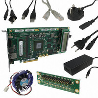
... Before using the kit or installing the software, check the kit contents and inspect the board to verify that you received all of the items listed in If any of the items are missing, contact Altera before you proceed. Inspect the Board To inspect the board, perform the following steps: 1 ...
Page 10
... References Use the following links to check the Altera website for other related information: ■ For the latest board design files and reference designs, refer to the FPGA Development Kit, 6G Edition ■ For additional daughter cards available for purchase, refer to the Board Daughtercards ■ ...
Page 11
... If you have difficulty installing the Quartus II software, refer to Installation and Licensing Considerations Purchasing this kit entitles you to a one-year DKE license for the Quartus II Subscription Edition Software. Before using the Quartus II software, you must activate your license, identify specific users and computers, and obtain and install a license file ...
Page 12
... NIC ID. Your NIC ID is the 12- digit hexadecimal number on the Physical Address line. 4. When licensing is complete, Altera emails a license.dat file to you. Store the file on your computer and use the License Setup page of the Options dialog box in the Quartus_II software to enable the software ...
Page 13
... USB-Blaster driver on the host computer. f Installation instructions for the USB-Blaster driver for your operating system are available on the Altera website. On the page of the Altera website, locate the table entry for your configuration and click the link to access the instructions. July 2010 Altera Corporation Figure 3– ...
Page 14
... Arria II GX FPGA Development Kit, 6G Edition User Guide Chapter 3: Software Installation Installing the USB-Blaster Driver July 2010 Altera Corporation ...
Page 15
... Arria II GX device configured successfully. f For more information about the PFL megafunction, refer to Loader with the Quartus II July 2010 Altera Corporation 4. Development Board Setup “Factory Default Switch Settings” on page 4–2 shows the switch location on the Arria II GX FPGA development Software ...
Page 16
... User DIP Switch OFF = SW2 PCIe MODE DIP Switch SW3 Table 4–1 and Function Chapter 4: Development Board Setup Factory Default Switch Settings Board Settings DIP Switch OFF = SW4 Figure 4–1. Default Position Off July 2010 Altera Corporation ...
Page 17
... This jumper has the following options: J9 pins 3-4 HSMA DIS Installing the shunt removes HSMC port A from the JTAG chain. ■ Removing the shunt includes HSMC port A in the JTAG chain. ■ July 2010 Altera Corporation Table 4–2 and Figure 4–1. Function Table 4–3 ...
Page 18
... For more information about the FPGA board settings, refer to the Development Board, 6G Edition Reference Arria II GX FPGA Development Kit, 6G Edition User Guide Chapter 4: Development Board Setup Factory Default Switch Settings Function Arria II GX FPGA Manual. July 2010 Altera Corporation Default Shunt Position Installed Installed ...
Page 19
... IP address from any DHCP server and serve a web page from the flash on your board to any host computer on the same network. The web page allows you to upload new FPGA designs to the user hardware 1 portion of flash memory, and provides links to useful information on the Altera website, including links to kit-specific and design resources. 1 After successfully updating the user hardware 1 flash memory, you can load the user design from flash memory into the FPGA ...
Page 20
... Board Update Portal web page the Hardware File Name field specify the .flash file that you either downloaded from the Altera website or created on your own. If there is a software component to the design, specify it in the same manner using the Software File Name field, otherwise leave the Software File Name field blank ...
Page 21
... The application allows you to exercise most of the board components. While using the application, you reconfigure the FPGA several times with test designs specific to the functionality you are testing. July 2010 Altera Corporation 6. Board Test System 3–2. Arria II GX FPGA Development Kit, 6G Edition User Guide ...
Page 22
... JTAG bus to the MAX II device, you can measure the power of any design in the FPGA, including your own designs. Arria II GX FPGA Development Kit, 6G Edition User Guide Chapter 6: Board Test System Figure 6–1 shows the initial GUI for a board that is July 2010 Altera Corporation Introduction ...
Page 23
... BoardTestSystem.exe application Windows, click Start > All Programs > Altera > Arria II GX FPGA Development Kit, 6G Edition <version> > Board Test System to run the application. A GUI appears, displaying the application tab that corresponds to the design running in the FPGA. The Arria II GX FPGA development board, 6G edition’s flash memory ships preconfigured with the design that corresponds to the Config, GPIO, and SRAM& ...
Page 24
... The Board information controls display static information about your board. Arria II GX FPGA Development Kit, 6G Edition User Guide “The Configure Menu” for information about configuring shows the Config tab. The tab displays the contents of the Chapter 6: Board Test System Using the Board Test System July 2010 Altera Corporation ...
Page 25
... MAX II ver—Indicates the version of MAX II code currently running on the board. The MAX II code resides in the <install dir>\kits\arriaIIGX_2agx260_fpga\examples directory. Newer revisions of this code might be available on the page of the Altera website. ■ MAC—Indicates the MAC address of the board. MAX II Registers ...
Page 26
... Arria II GX FPGA Development Kit, 6G Edition User Guide Chapter 6: Board Test System Using the Board Test System Table 6–1 Table 6–1 for the list of Table 6–1 for the list of available Table 6–1 for more information. July 2010 Altera Corporation ...
Page 27
... The read-only User DIP switches control displays the current positions of the switches in the user DIP switch bank (SW3). Change the switches on the board to see the graphical display change accordingly. July 2010 Altera Corporation Figure 6–3 shows the GPIO tab. Arria II GX FPGA Development Kit, 6G Edition User Guide ...
Page 28
... Figure 6–4 Figure 6–4. The SRAM&Flash Tab The following sections describe the controls on the SRAM&Flash tab. Arria II GX FPGA Development Kit, 6G Edition User Guide shows the SRAM&Flash tab. Chapter 6: Board Test System Using the Board Test System July 2010 Altera Corporation ...
Page 29
... To prevent overwriting the dedicated portions of flash memory, the application limits the writable flash memory address range from 0x03FE.0000 to 0x003F.FFFF (which corresponds to the unused flash memory address range shown in page 6–2 and July 2010 Altera Corporation Table A–1 on page A–1). Arria II GX FPGA Development Kit, 6G Edition User Guide 6–9 ...
Page 30
... The Stop control terminates transaction performance analysis. Performance Indicators These controls display current transaction performance analysis information collected since you last pressed Start: Arria II GX FPGA Development Kit, 6G Edition User Guide Chapter 6: Board Test System Using the Board Test System July 2010 Altera Corporation ...
Page 31
... Write then read—Selects read and write transactions for analysis. ■ Read only—Selects read transactions for analysis. ■ Write only—Selects write transactions for analysis. July 2010 Altera Corporation Arria II GX FPGA Development Kit, 6G Edition User Guide 6–11 ...
Page 32
... The Stop control terminates transaction performance analysis. Performance Indicators These controls display current transaction performance analysis information collected since you last clicked Start: Arria II GX FPGA Development Kit, 6G Edition User Guide Chapter 6: Board Test System Using the Board Test System July 2010 Altera Corporation ...
Page 33
... Write/Read—Selects read and write transactions for analysis. ■ Read Only—Selects read transactions for analysis. ■ Write Only—Selects write transactions for analysis. July 2010 Altera Corporation Arria II GX FPGA Development Kit, 6G Edition User Guide 6–13 ...
Page 34
... Pattern sync—Shows the pattern synced or not synced state. The pattern is considered synced when the start of the data sequence is detected. Arria II GX FPGA Development Kit, 6G Edition User Guide shows the HSMC tab. Chapter 6: Board Test System Using the Board Test System July 2010 Altera Corporation ...
Page 35
... These controls display current transaction performance analysis information collected since you last clicked Start: ■ TX and RX performance bars—Show the percentage of maximum theoretical data rate that the requested transactions are able to achieve. July 2010 Altera Corporation Arria II GX FPGA Development Kit, 6G Edition User Guide 6–15 ...
Page 36
... You can also run the Power Monitor as a stand-alone application. PowerMonitor.exe resides in the <install dir>\kits\arriaIIGX_2agx260_fpga\examples\board_test_system directory. On Windows, click Start > All Programs > Altera > Arria II GX FPGA Development Kit, 6G Edition <version> > Power Monitor to start the application. Arria II GX FPGA Development Kit, 6G Edition User Guide ...
Page 37
... Newer revisions of this code might be available on the Edition page of the Altera website. Power rail—Selects the power rail to measure. After selecting the desired rail, click ■ Reset to refresh the screen with new board readings. ...
Page 38
... The first measurement is Vsense and the difference between the two measurements is Vdif. Plug the values into the equation to determine the power consumption. Arria II GX FPGA Development Kit, 6G Edition User Guide Chapter 6: Board Test System The Power Monitor Arria II GX FPGA Manual. July 2010 Altera Corporation ...
Page 39
... Using the Quartus II programmer to configure a device on the board causes other JTAG-based applications such as the Board Test System and the Power Monitor to loose their connection to the board. Restart those applications after configuration is complete. July 2010 Altera Corporation Arria II GX FPGA Development Kit, 6G Edition User Guide 6–19 ...
Page 40
... Arria II GX FPGA Development Kit, 6G Edition User Guide Chapter 6: Board Test System Configuring the FPGA Using the Quartus II Programmer July 2010 Altera Corporation ...
Page 41
... Introduction As you develop your own project using the Altera tools, you can program the flash memory device so that your own design loads from flash memory into the FPGA on power up. This appendix describes the preprogrammed contents of the common flash interface (CFI) flash memory device on the Arria II GX FPGA development board, 6G edition and the Nios II EDS tools involved with reprogramming the user portions of the flash memory device ...
Page 42
... If you have an FPGA design developed using the Quartus II software, and software developed using the Nios II EDS, follow these instructions the Windows Start menu, click All Programs > Altera > Nios II EDS > Nios II Command Shell the Nios II command shell, navigate to the directory where your design files reside and type the following Nios II EDS commands: For Quartus II ...
Page 43
... The CONF DONE LED (D14) and the four user LEDs (D7-D10) illuminate indicating that the flash device is ready for programming the Windows Start menu, click All Programs > Altera > Nios II EDS > Nios II Command Shell the Nios II command shell, navigate to the <install dir> ...
Page 44
... The CONF DONE LED (D14) and the four user LEDs (D7-D10) illuminate indicating that the flash device is ready for programming the Windows Start menu, click All Programs > Altera > Nios II EDS > Nios II Command Shell the Nios II command shell, navigate to the <install dir> ...
Page 45
... To ensure that you have the most up-to-date factory restore files and information about this product, refer to the of the Altera website. July 2010 Altera Corporation Arria II GX FPGA Development Kit, 6G Edition 4–2. Arria II GX FPGA Development Kit, 6G Edition Arria II GX FPGA Development Kit, 6G Edition User Guide A– ...
Page 46
... A–6 Arria II GX FPGA Development Kit, 6G Edition User Guide Chapter : Restoring the MAX II CPLD to the Factory Settings July 2010 Altera Corporation ...
Page 47
... Technical training Product literature Non-technical support (General) (Software Licensing) Note to Table: (1) You can also contact your local Altera sales office or sales representative. Typographic Conventions The following table shows the typographic conventions this document uses. Visual Cue Bold Type with Initial Capital ...
Page 48
... A warning calls attention to a condition or possible situation that can cause you injury. The envelope links to the Email Subscription Management Center website, where you can sign up to receive update notifications for Altera documents. Additional Information Typographic Conventions page of the Altera July 2010 Altera Corporation ...