DO-CPLD-DK-G Xilinx Inc, DO-CPLD-DK-G Datasheet
DO-CPLD-DK-G
Specifications of DO-CPLD-DK-G
Available stocks


Related parts for DO-CPLD-DK-G


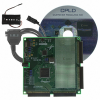
DO-CPLD-DK-G Summary of contents
Page 1
R DS063 (v5.5) June 25, 2007 Features • High-performance - 5 ns pin-to-pin logic delays on all pins - f to 125 MHz CNT • Large density range - 36 to 288 macrocells with 800 to 6,400 usable gates ...
Page 2
XC9500 In-System Programmable CPLD Family Table 2: Available Packages and Device I/O Pins (not including dedicated JTAG pins) XC9536 44-Pin VQFP 34 44-Pin PLCC 34 48-Pin CSP 34 84-Pin PLCC - 100-Pin TQFP - 100-Pin PQFP - 160-Pin PQFP - ...
Page 3
R associated output enable signals drive directly to the IOBs. See Figure 1. 3 JTAG Port I/O I/O I/O I/O I/O I/O I/O I/O 3 I/O/GCK 1 I/O/GSR I/O/GTS Note: Function block outputs (indicated by the bold ...
Page 4
XC9500 In-System Programmable CPLD Family From 36 Fast CONNECT II Switch Matrix 4 Macrocell 1 Product Programmable Term AND-Array Allocators Macrocell 18 1 Global Set/Reset Figure 2: XC9500 Function Block www.xilinx.com 18 To Fast CONNECT II Switch Matrix 18 OUT ...
Page 5
R Macrocell Each XC9500 macrocell may be individually configured for a combinatorial or registered function. The macrocell and associated FB logic is shown in Figure Five direct product terms from the AND-array are available for use as primary data inputs ...
Page 6
XC9500 In-System Programmable CPLD Family All global control signals are available to each individual macrocell, including clock, set/reset, and output enable sig- nals. As shown in Figure 4, the macrocell register clock originates from either of three global clocks or ...
Page 7
R Product Term Allocator The product term allocator controls how the five direct prod- uct terms are assigned to each macrocell. For example, all five direct terms can drive the OR function as shown in Figure 5. Product Term Allocator ...
Page 8
XC9500 In-System Programmable CPLD Family The product term allocator can re-assign product terms from any macrocell within the FB by combining partial sums of products over several macrocells, as shown in In this example, the incremental delay is only 2 ...
Page 9
R The internal logic of the product term allocator is shown in Figure 8. From Upper Macrocell From Lower Macrocell DS063 (v5.5) June 25, 2007 Product Specification XC9500 In-System Programmable CPLD Family To Upper Macrocell Product Term Allocator To Lower ...
Page 10
XC9500 In-System Programmable CPLD Family Fast CONNECT Switch Matrix The Fast CONNECT switch matrix connects signals to the FB inputs, as shown in Figure 9. All IOB outputs (corre- sponding to user pin inputs) and all FB outputs drive the ...
Page 11
... Product Specification XC9500 In-System Programmable CPLD Family 5V voltage supply (V olds are constant and do not vary with the V The output enable may be generated from one of four options: a product term signal from the macrocell, any of the global OE signals, always [1], or always [0]. There are two ...
Page 12
... XC9500 In-System Programmable CPLD Family Each output has independent slew rate control. Output edge rates may be slowed down to reduce system noise (with an additional time delay of T SLEW ming. See Figure 11. Each IOB provides user programmable ground pin capabil- ity. This allows device I/O pins to be configured as additional ground pins ...
Page 13
... JTAG instruction sequence. All I/Os are 3-stated and pulled high by the IOB resistors during in-system programming particular signal must remain Low during this time, then a pulldown resistor may be added to the pin. External Programming XC9500 devices can also be programmed by the Xilinx HW130 device programmer as well as third-party program- mers ...
Page 14
... XC9500 In-System Programmable CPLD Family Figure 13: In-System Programming Operation (a) Solder Device to PCB and (b) Program Using Download Cable Low Power Mode All XC9500 devices offer a low-power mode for individual macrocells or across all macrocells. This feature allows the device power to be significantly reduced. ...
Page 15
R Combinatorial Logic Propagation Delay = T (a) T PSU Combinatorial Logic P-Term Clock Path Setup Time = T PSU (c) All resources within FB using local Feedback Combinatorial Logic Internal Cycle Time = T ( GCK ...
Page 16
... Device Outputs 16 implement the design and generate a JEDEC bitmap which can be used to program the XC9500 device. Each develop- ment system includes JTAG download software that can be used to program the devices via the standard JTAG inter- face and a download cable. FastFLASH Technology An advanced CMOS Flash process is used to fabricate all XC9500 devices ...
Page 17
... Warranty Disclaimer THESE PRODUCTS ARE SUBJECT TO THE TERMS OF THE XILINX LIMITED WARRANTY WHICH CAN BE VIEWED AT http://www.xilinx.com/warranty.htm. THIS LIMITED WARRANTY DOES NOT EXTEND TO ANY USE OF THE PRODUCTS IN AN APPLICATION OR ENVIRONMENT THAT IS NOT WITHIN THE SPECIFICATIONS STATED ON THE THEN-CURRENT XILINX DATA SHEET FOR THE PRODUCTS. PRODUCTS ARE NOT DESIGNED TO BE FAIL-SAFE AND ARE NOT WARRANTED FOR USE IN APPLICATIONS THAT POSE A RISK OF PHYSICAL HARM OR LOSS OF LIFE ...