HW-V5-ML506-UNI-G Xilinx Inc, HW-V5-ML506-UNI-G Datasheet - Page 28
HW-V5-ML506-UNI-G
Manufacturer Part Number
HW-V5-ML506-UNI-G
Description
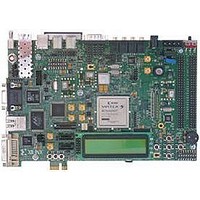
EVALUATION PLATFORM VIRTEX-5
Manufacturer
Xilinx Inc
Series
Virtex™-5 SXTr
Type
DSPr
Datasheet
1.HW-V5-ML507-UNI-G.pdf
(60 pages)
Specifications of HW-V5-ML506-UNI-G
Contents
Evaluation Platform, DVI Adapter and CompactFlash Card
Silicon Manufacturer
Xilinx
Features
JTAG Programming Interface, Platform Flash, External Clocking
Kit Contents
Board, Cable, PSU, CD, Docs
Silicon Family Name
Virtex-5
Silicon Core Number
XC5VSX50TFFG1136
Rohs Compliant
Yes
Lead Free Status / RoHS Status
Lead free / RoHS Compliant
For Use With/related Products
XC5VSX50TFFG1136
Lead Free Status / RoHS Status
Lead free / RoHS Compliant, Lead free / RoHS Compliant
Available stocks
Company
Part Number
Manufacturer
Quantity
Price


Chapter 1: ML505/ML506/ML507 Evaluation Platform
28
16. PS/2 Mouse and Keyboard Ports
17. System ACE and CompactFlash Connector
The DVI connector
monitor’s configuration parameters. These parameters can be read by the FPGA using the
VGA IIC bus.
Table 1-14: DVI Controller Connections
The board contains two PS/2 ports: one for a mouse (P5) and the other for a keyboard (P4).
Bidirectional level shifting transistors allow the FPGA's 1.8V I/O to interface with the 5V
I/O of the PS/2 ports. The PS/2 ports on the board are powered directly by the main 5V
power jack, which also powers the rest of the board.
The Xilinx System ACE CompactFlash (CF) configuration controller allows a Type I
CompactFlash card to program the FPGA through the JTAG port. Both hardware and
software data can be downloaded through the JTAG port. The System ACE controller
supports up to eight configuration images on a single CompactFlash card. The
configuration address switches allow the user to choose which of the eight configuration
images to use.
DVI_D[0]
DVI_D[1]
DVI_D[2]
DVI_D[3]
DVI_D[4]
DVI_D[5]
DVI_D[6]
DVI_D[7]
DVI_D[8]
DVI_D[9]
DVI_D[10]
DVI_D[11]
DVI_XCLK_P
DVI_XCLK_N
DVI_HSYNC
DVI_VSYNC
DVI_DE
DVI_RESET_B
Caution!
not overload the AC adapter.
Net Name
Care must be taken to ensure that the power load of any attached PS/2 devices does
(Table
www.xilinx.com
1-14) supports the IIC protocol to allow the board to read the
FPGA Pin
AM13
AM12
AM11
AN12
AN13
AA10
AN14
AP12
AB10
AP14
AL10
AL11
AC8
AA9
AA8
AK6
AB8
AE8
ML505/ML506/ML507 Evaluation Platform
UG347 (v3.1.1) October 7, 2009
R
Related parts for HW-V5-ML506-UNI-G
Image
Part Number
Description
Manufacturer
Datasheet
Request
R

Part Number:
Description:
IC CPLD .8K 36MCELL 44-VQFP
Manufacturer:
Xilinx Inc
Datasheet:

Part Number:
Description:
IC CPLD 72MCRCELL 10NS 44VQFP
Manufacturer:
Xilinx Inc
Datasheet:

Part Number:
Description:
IC CPLD 1.6K 72MCELL 64-VQFP
Manufacturer:
Xilinx Inc
Datasheet:

Part Number:
Description:
IC CR-II CPLD 64MCELL 44-VQFP
Manufacturer:
Xilinx Inc
Datasheet:

Part Number:
Description:
IC CPLD 1.6K 72MCELL 100-TQFP
Manufacturer:
Xilinx Inc
Datasheet:

Part Number:
Description:
IC CR-II CPLD 64MCELL 56-BGA
Manufacturer:
Xilinx Inc
Datasheet:

Part Number:
Description:
IC CPLD 72MCRCELL 7.5NS 44VQFP
Manufacturer:
Xilinx Inc
Datasheet:
Part Number:
Description:
IC CR-II CPLD 64MCELL 100-VQFP
Manufacturer:
Xilinx Inc
Datasheet:
Part Number:
Description:
IC CPLD 1.6K 72MCELL 100-TQFP
Manufacturer:
Xilinx Inc
Datasheet:

Part Number:
Description:
IC CPLD 72MCRCELL 7.5NS 64VQFP
Manufacturer:
Xilinx Inc
Datasheet:
Part Number:
Description:
IC CPLD 1.6K 72MCELL 100-TQFP
Manufacturer:
Xilinx Inc
Datasheet:

Part Number:
Description:
IC CPLD 1.5K 64MCELL HP 44-VQFP
Manufacturer:
Xilinx Inc

Part Number:
Description:
IC CPLD 36MCRCELL 15NS 44PLCC
Manufacturer:
Xilinx Inc
Datasheet:

Part Number:
Description:
IC CPLD 36MCRCELL 10NS 44PLCC
Manufacturer:
Xilinx Inc
Datasheet:

Part Number:
Description:
IC CPLD 1.5K 64MCELL HP 44-VQFP
Manufacturer:
Xilinx Inc