HW-V5-ML550-UNI-G Xilinx Inc, HW-V5-ML550-UNI-G Datasheet
HW-V5-ML550-UNI-G
Specifications of HW-V5-ML550-UNI-G
Available stocks


Related parts for HW-V5-ML550-UNI-G


HW-V5-ML550-UNI-G Summary of contents
Page 1
Virtex-5 FPGA ML550 Networking Interfaces Platform User Guide UG202 (v1.4) April 18, 2008 R ...
Page 2
Xilinx is disclosing this user guide, manual, release note, and/or specification (the "Documentation") to you solely for use in the development of designs to operate with Xilinx hardware devices. You may not reproduce, distribute, republish, download, display, post, or transmit ...
Page 3
Table of Contents Preface: About This Guide Guide Contents . . . . . . . . . . . . . . . . . . . . . . . . . . . . . . . ...
Page 4
Important Note About ± 5% Margin Limits Power Monitor Connector ML550 System Monitor and Power Monitor Support ML550 Board System Monitor Support Circuitry Details . . . . . . . . . . . . . . . . ...
Page 5
R Appendix D: ML550 Starter UCF UCF Starter File . . . . . . . . . . . . . . . . . . . . . . . . . . . . . . . ...
Page 6
ML550 Networking Interfaces Platform R UG202 (v1.4) April 18, 2008 ...
Page 7
R About This Guide This user guide is a description of the Virtex Development Board. Complete and up-to-date documentation of the Virtex-5 family of FPGAs is available on the Xilinx website at http://www.xilinx.com/virtex5. Guide Contents This manual contains the following ...
Page 8
Preface: About This Guide - SelectIO Logic Resources - Advanced SelectIO Logic Resources Virtex-5 FPGA RocketIO GTP Transceiver User Guide This guide describes the RocketIO™ GTP transceivers available in the Virtex-5 LXT and SXT platforms. Virtex-5 FPGA RocketIO GTX Transceiver ...
Page 9
R Typographical Conventions This document uses the following typographical conventions. An example illustrates each convention. Convention Italic font Underlined Text Online Document The following conventions are used in this document: Convention Blue text Red text Blue, underlined text ML550 Networking ...
Page 10
Preface: About This Guide 10 www.xilinx.com ML550 Networking Interfaces Platform R UG202 (v1.4) April 18, 2008 ...
Page 11
R Introduction About the Virtex-5 FPGA Source-Synchronous Interfaces Tool Kit ® The Virtex development platform for designing and verifying applications based on the Virtex-5 LXT FPGA family. This kit allows designers to implement high-speed applications with extreme flexibility using IP ...
Page 12
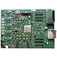
Chapter 1: Introduction Virtex-5 FPGA ML550 Networking Interfaces Development Board The ML550 Development Board includes the following: XC5VLX50T-FFG1136 FPGA 64M x 8 DDR SDRAM memory Eight clock sources: 200 MHz, 250 MHz, 133 MHz, and 33 MHz on-board oscillators Two ...
Page 13
R Figure 1-1 shows the ML550 Development Board. Graphic 64 x 128 LCD USB “B” Connector (Under LCD) System ACE Reset and Configuration Switches LVDS Receive Connectors XC5VLX50TFF1136 FPGA 250-MHz Oscillator Power Monitor Header External Clock Input SMAs 64-MB DDR ...
Page 14
Chapter 1: Introduction 14 www.xilinx.com ML550 Networking Interfaces Platform R UG202 (v1.4) April 18, 2008 ...
Page 15
R Getting Started This chapter describes the items needed to configure the Virtex-5 FPGA ML550 Networking Interfaces Development Board. The ML550 Development Board is tested at the factory after assembly and should be received in working condition set ...
Page 16
Chapter 2: Getting Started Plug the 5V power supply line cord into a power outlet, and plug the barrel plug into the ML550 J20 jack. Plug the “B” end of the kit USB cable into the ML550 (the jack is ...
Page 17
R BERT GUI Tcl Interface Installation 1. Locate executable file ActiveTcl8.4.7.0-win32-ix86-108887.exe in C:\ML550 BERT REV1.x and double-click on it. 2. The Active State Active Tcl installer opens. Follow the dialog and accept the defaults. At the end of the process, ...
Page 18
Chapter 2: Getting Started Select change to COM# where # is either 10. The GUI reflects the frequency set at Clock Module 2 and initially reports 400 MHz. More information resides in the file C:\ML550 ...
Page 19
R Hardware Description A high-level block diagram of the Virtex-5 FPGA ML550 Networking Interfaces Development Board is shown in section. 250 MHz, 200 MHz 133 MHz, 33 MHz Clock Synthesizers Clock Generator Figure 3-1: Virtex-5 FPGA ML550 Networking Interfaces Development ...
Page 20
Chapter 3: Hardware Description Clock Generation The clock generation section of the ML550 Development Board provides all necessary clocks for the Virtex-5 FPGA. Eight clock sources are provided: Epson EG2121CA 2.5V 250-MHz differential LVPECL oscillator (Y4) for general use Epson ...
Page 21
R SDRAM Memory The ML550 Development Board provides 64 MBytes of SDRAM memory (Micron Semiconductor MT46V64M8BN-75). The high-level block diagram of the SDRAM interface is shown in FFG1136 package used on the ML550 Development Board. Table 3-2: SDRAM Memory Interface ...
Page 22
Chapter 3: Hardware Description Table 3-2: SDRAM Memory Interface Signal Descriptions (Continued) Signal Name DQ2 DQ3 DQ4 DQ5 DQ6 DQ7 (1) DQS0 BA0 BA1 DM0 CSn RASn CASn WEn CLK_P CLK_N CKE Notes: 1. Because DQS0 is not located on ...
Page 23
R Table 3-3: LCD Interface Signal Descriptions (Continued) Signal Name DB6 DB5 DB4 DB3 DB2 DB1 DB0 E R/W RS RST CS1B LED + LED – LCD_BL_ON The LCD can display alphanumeric (ASCII) information; however, a hardware character generator must ...
Page 24
Chapter 3: Hardware Description A 64-step electronic contrast control function Table 3-4 summarizes the controller specifications. Table 3-4: Display Controller Specifications Parameter Supply Voltage LCD Driving Voltage Power Consumption Sleep Mode Standby Mode Hardware Schematic Diagrams Figure 3-3 diagram of ...
Page 25
DB1 11 DB0 R RST 16 CS1B 17 LED 18 LED 2.50 2.54 User LED The ML550 Development Board provides six user ...
Page 26
Chapter 3: Hardware Description Table 3-5: User LED Pin Assignments USER_LED1 USER_LED2 USER_LED3 USER_LED4 USER_LED5 USER_LED6 Configuration INIT and DONE LEDs The ML550 Development Board provides an INIT LED and a DONE LED, which are activated by drive transistors responding ...
Page 27
R Program Switch The ML550 Development Board provides a push-button program switch (SW12) for initiating the configuration of the Virtex-5 FPGA. This switch is used to force a reconfiguration of the FPGA from PROMs if they are present and enabled. ...
Page 28
Chapter 3: Hardware Description A high-level block diagram of the USB interface is shown in cable included in the kit mates with the J22 connector. U2 USB_D- 5 USB_VBUS GND 3 USB_D+ 4 CP2102 LVDS ...
Page 29
... LVDS Loopback Board (Xilinx P/N 0431395) LVDS transmit to receive loopback can be achieved with either the LVDS Loopback board included in the kit, or with the Precision Interconnect Blue Ribbon Cables (Xilinx P/N HW-LVDS-CBL-80, order separately). LVDS Loopback Board details. Voltage Regulators (TI PTH05000) Figure 3-7 various on-board voltage sources ...
Page 30
Chapter 3: Hardware Description Jumper OFF = Enabled Jumper ON = Inhibited The TI PTH05000 regulator module requires a fixed 5V input. The output is adjustable over a range of 0.9V to 3.6V by changing the resistor tied between pin ...
Page 31
R Table 3-11: VR_SEL[3:0] FPGA Pinout VR_SEL[3:0] VR_SEL0 VR_SEL1 VR_SEL2 VR_SEL3 The ML550 Networking Interfaces Platform implements the remote ±5% output adjustment using two Maxim analog mux devices: an 8-to-1 for the margin R and a 2-to-1 to select between ...
Page 32
Chapter 3: Hardware Description Margin Control Data Latch V CC U25 VR_SEL0 VR_SEL1 VR_SEL2 VR_SEL3 STB_VCCINT1V0 9 3 CLK 1Q FPGA_RESETB ...
Page 33
R voltage taps on each resistor are wired to the P72 Power Monitor connector. shows a typical current sense resistor topology this case, V connected to the “input” side Kelvin resistor. The “output” ...
Page 34
Chapter 3: Hardware Description ML550 System Monitor and Power Monitor Support The Virtex-5 FPGA System Monitor block diagram is shown in VAUXP[0] VAUXN[0] VAUXP[14] VAUXN[14] VAUXP[15] VAUXN[15] Temperature V CCINT V CCAUX V REFP V REFN Internal Supplies The ML550 ...
Page 35
R Table 3-13: ML550 System Monitor Connections (Continued) System Monitor FPGA Parameter Measured Input Channel Pin# VAUXN[14] K32 5V Current (N) VAUXP[14] K33 5V Current (P) VAUXN[15] K34 PCB Temperature (N) VAUXP[15] L34 PCB Temperature (P) VN V17 J19.3 connector ...
Page 36
Chapter 3: Hardware Description ML550 Board System Monitor Support Circuitry Details Figure 3-12 device, and pin number the indicated signal connects: S#,Des.P# where the schematic sheet number (for example, 19) Des is the device reference designator (for example, ...
Page 37
R 2.5V V CCAUX The signal conditioning network is shown in VCC2V5_VAUX C139 0.001µF 2.5V V Voltage Monitor CCO The signal conditioning network is shown in VCC2V5_VCCO C120 0.001µF ML550 Networking Interfaces Platform UG202 (v1.4) April 18, 2008 ML550 System ...
Page 38
Chapter 3: Hardware Description 2.5V System Power Voltage Monitor The signal conditioning network is shown in VCC2V5 C70 0.001µF 1.0V V Voltage Monitor CCINT The signal conditioning network is shown in VCC1V0 C32 0.001µF 38 Figure 2 R121 R274 10.0K ...
Page 39
R 5V Input Power Current Monitor The signal conditioning network is shown in SMV internal connections: 1 & & 4 MEASURED_5V from 5V input network 21,F1.2 21,R197.2 1 R200 10. C151 0.1µF 2 Gain Jumper: 1 ...
Page 40
Chapter 3: Hardware Description 2.5V V System Monitor REF The signal conditioning network is shown in VCC2V5_VAUX HDR_1X3_RA P39 L2 3 HZ0805E601R- SM_AVDD 30,U9.T18 30,J19.8 REF_2V5_OUT 19,U11.4 30,J19.7 L1 HZ0805E601R-00 SM_VREF_P 30,U9.V18 1 Figure 3-19: System Monitor 2.5V ...
Page 41
R J19 Mezzanine Board Connector J19 is provided to enable users to develop signal conditioning boards and take advantage of the System Monitor VP/VN input channel on FPGA pins U18/V17. The J19 connections to the FPGA are shown in to ...
Page 42
Chapter 3: Hardware Description Table 3-15: J19 Mezzanine Board Connector Pin # REF_2V5_OUT Figure 3-21 23,R386.2 23,R189.2 24,R384.2 24,R220.2 22,R385.2 22,R187.2 22,R383.2 22,R163.2 ...
Page 43
R Power Monitor Circuitry The ML550 hosts 0.1-inch male header connector which provides test points for the ML550 power regulators as shown in Table 3-16: Power Monitor Connector P72 Pinout Pin # ...
Page 44
Chapter 3: Hardware Description Power Monitor Board A small PC board (1.375 inches x 2.25 inches) is available which mates with P72 and provides two banana jacks for voltmeter probe access to V Figure 3-22. Data Sheet References Table 3-17 ...
Page 45
R Configuration The Virtex-5 FPGA ML550 Networking Interfaces Development Board includes several options to configure the Virtex-5 FPGA. The configuration modes are: System ACE mode JTAG mode Slave Serial mode Master Serial mode This chapter provides a brief description of ...
Page 46
Chapter 4: Configuration JTAG Chain Figure 4-2 three different sources can be used to drive this JTAG chain. The chain can be driven by the following sources: System ACE controller Xilinx Parallel Cable IV or Platform Cable USB Other JTAG ...
Page 47
R JTAG Ports The ML550 Development Board provides two JTAG connectors (P50 and P51) that can be used to program the Virtex-5 FPGA. connectors P50. Table 4-2 describes the P50 JTAG Header signal names, descriptions, and pin assignments. Table 4-2: ...
Page 48
Chapter 4: Configuration 2 mm Flat Cable Port The ML550 Development Board provides flat cable connector (P51) to configure the Virtex-5 FPGA. The 2 mm flat cable connector can also be used to configure the FPGA in ...
Page 49
R System ACE Interface The ML550 Development Board provides a System ACE interface to configure the Virtex-5 FPGA. The interface also gives software designers the ability to run code (for soft processor IP within the FPGA) from removable CompactFlash cards. ...
Page 50
Chapter 4: Configuration Table 4-3 shows the System ACE interface signal names, descriptions, and pin assignments. Table 4-3: System ACE Interface Signal Descriptions System ACE Pin Number ...
Page 51
R LVDS This appendix provides the pinouts for the six LVDS connectors. LVDS Transmit Connectors Table A-1 lists the connections for LVDS transmit connector #1 (P73), connections for LVDS transmit connector #2 (P46), and LVDS transmit connector #3 (P49). These ...
Page 52
Appendix A: LVDS Table A-1: LVDS Transmit Connector #1 (P73) (Continued) P73 TX Signal Name Pin # 17 GND 18 GND GND 24 GND LVDS_DATAOUT_18N ...
Page 53
R Table A-2: LVDS Transmit Connector #2 (P46) P46 TX Signal Name Pin # GND 6 GND GND 12 GND 13 NC ...
Page 54
Appendix A: LVDS Table A-2: LVDS Transmit Connector #2 (P46) (Continued) P46 TX Signal Name Pin # 33 LVDS_DATAOUT_35P 34 XMITCLK_P 35 GND 36 GND 37 LVDS_DATAOUT_33N 38 LVDS_DATAOUT_34N 39 LVDS_DATAOUT_33P 40 LVDS_DATAOUT_34P 41 LVDS_DATAOUT_31N 42 LVDS_DATAOUT_32N 43 LVDS_DATAOUT_31P 44 ...
Page 55
R Table A-3: LVDS Transmit Connector #3 (P49) (Continued) P49 TX Signal Name Pin # 18 GND GND 24 GND GND 30 ...
Page 56
Appendix A: LVDS LVDS Receive Connectors Table A-4 lists the connections for LVDS receive connector #1 (P74), connections for LVDS receive connector #2 (P6), and LVDS receive connector #3 (P3). These connectors and their associated FPGA banks are detailed on ...
Page 57
R Table A-4: LVDS Receive Connector #1 (P74) (Continued) P74 RX Signal Name Pin # 27 LVDS_DATAIN_CLKCAP_08N 28 LVDS_DATAIN_CLKCAP_09N 29 GND 30 GND 31 LVDS_DATAIN_CLKCAP_10P 32 LVDS_DATAIN_CLKCAP_11P 33 LVDS_DATAIN_CLKCAP_10N 34 LVDS_DATAIN_CLKCAP_11N 35 GND 36 GND 37 LVDS_DATAIN_12P 38 LVDS_DATAIN_13P 39 ...
Page 58
Appendix A: LVDS Table A-5: LVDS Receive Connector #2 (P6) (Continued Signal Name Pin # 12 GND 13 LVDS_DATAIN_24P 14 LVDS_DATAIN_23P 15 LVDS_DATAIN_24N 16 LVDS_DATAIN_23N 17 GND 18 GND 19 LVDS_DATAIN_26P 20 LVDS_DATAIN_25P 21 LVDS_DATAIN_26N 22 LVDS_DATAIN_25N 23 ...
Page 59
R Table A-5: LVDS Receive Connector #2 (P6) (Continued Signal Name Pin # 43 LVDS_DATAIN_34N 44 LVDS_DATAIN_33N Table A-6: LVDS Receive Connector #3 (P3 Signal Name Pin # 1 LVDS_DATAIN_36P LVDS_DATAIN_36N 4 NC ...
Page 60
Appendix A: LVDS Table A-6: LVDS Receive Connector #3 (P3) (Continued Signal Name Pin # 28 LVDS_DATAIN_CLKCAP_43N 29 GND 30 GND 31 LVDS_DATAIN_46P 32 LVDS_DATAIN_45P 33 LVDS_DATAIN_46N 34 LVDS_DATAIN_45N 35 GND 36 GND 37 LVDS_DATAIN_48P 38 LVDS_DATAIN_47P 39 ...
Page 61
R LVDS Loopback Board The Xilinx LVDS Loopback board (P/N 0431395 ML550 accessory board that bridges the ML550 LVDS Transmit and Receive Samtec connectors. the board. The specifications for the loopback board are: Dimensions are 2.25 inches by ...
Page 62
Appendix B: LVDS Loopback Board 62 www.xilinx.com ML550 Networking Interfaces Platform R UG202 (v1.4) April 18, 2008 ...
Page 63
R LCD Interface This appendix is extracted from the XLVDSPRO Demonstration Boards User Guide (UG037). It describes the LCD interface for the XLVDSPRO demonstration boards, which is identical to that used in the ML550 Development Board. The documentation is reproduced ...
Page 64
Appendix C: LCD Interface Table C-1 summarizes the controller specifications. Table C-1: Display Controller Specifications Parameter Supply voltage LCD driving voltage Power consumption Sleep mode Standby mode The on-chip RAM size is 65x132 = 8580 bits. Hardware Schematic Diagram LCD-BUS ...
Page 65
R Peripheral Device KS0713 Figure C-2 sheet from the Samsung web pages for a complete signal listing. VDD VSS V/F Circuit V/R Circuit V/C Circuit KS0713 Samsung ML550 Networking Interfaces Platform UG202 (v1.4) April 18, 2008 shows only the signals ...
Page 66
Appendix C: LCD Interface DB1 11 DB0 R RST 16 CS1B 17 LED+ 18 LED- 2.50 2.54 66 VSS Jumper J3 VDD MI DB7 ...
Page 67
R Controller – Operation The pixels for the LCD panel are stored in the controller data RAM. This RAM is a 65-row by 132-column array. Each display pixel is represented by a single bit in the RAM array. The interface ...
Page 68
Appendix C: LCD Interface Table C-2: LCD Panel (Continued) DB3 DB2 DB1 DB0 Data DB0 DB1 DB2 DB3 DB4 DB5 DB6 DB7 DB0 DB1 DB2 DB3 DB4 DB5 DB6 DB7 DB0 DB1 ...
Page 69
R Table C-2: LCD Panel (Continued) DB3 DB2 DB1 DB0 Data DB0 DB1 DB2 DB3 DB4 DB5 DB6 DB7 DB0 DB1 DB2 DB3 DB4 DB5 DB6 DB7 DB0 ...
Page 70
Appendix C: LCD Interface Controller – LCD Panel Connections The controller die, KS0713, connects to the LCD glass panel and user connection pins via a small PCB. Other necessary pins have default connections on the PCB. how all pins of ...
Page 71
R Table C-3: KS0713 Pin Connections (Continued) Connector J1 Connector J2 Connection Voltage Converter and Control ML550 Networking Interfaces Platform UG202 (v1.4) April 18, 2008 PCB Signal Connected to Name OPEN DISP OPEN CL OPEN M OPEN FRS 18 VOUT ...
Page 72
Appendix C: LCD Interface Controller – Power Supply Circuits Figure C-5 boost mode, where VDD is 3.3V and VOUT is 16.5V. VOUT is the operating voltage of the operational amplifier delivering the operating voltage, V0, for the LCD panel. The ...
Page 73
R The voltage and contrast settings must be configured before the LCD panel is ready for operation. controller. ADC Select - ADC = 0 SEG1 --> SEG132 - ADC = 1 SEG132 --> SEG1 SHL Select - SHL = 0 ...
Page 74
Appendix C: LCD Interface Normal power mode is set The voltage follower and voltage regulator are set to: Five times boost mode The V4, V3, V2, V1, and V0 outputs depend on the bias settings of 1/9 or 1/7. Because ...
Page 75
R When SHL is set to 1, the common lines are scanned in opposite direction. Once configured, these settings normally are not changed. Select the LCD bias settings. The duty cycle is selected as 1/65 by hardwiring the controller IC ...
Page 76
Appendix C: LCD Interface Instruction Set Table C-7 shows the instruction set for the LCD panel. Table C-7: Display Instructions Instruction RS RW Read display data 1 8-bit data specified by the column and page address can be read from ...
Page 77
R Table C-7: Display Instructions (Continued) Instruction RS RW Set page address 0 This instruction sets the address of the display data page. Any RAM data bit can be accessed when its page address and column address are specified. Changing ...
Page 78
Appendix C: LCD Interface Table C-7: Display Instructions (Continued) Instruction RS RW Reverse display ON/OFF 0 Entire display ON/OFF 0 This instruction forces the display to be turned on regardless of the contents of the display data RAM. The contents ...
Page 79
R Read/Write Characteristics (6800 Mode) Table C-8: Read/Write Characteristics in 6800 Mode Parameter Address setup time Address hold time Data setup time Data hold time Access time Output disable time System cycle time Enable pulse width RS RW CS1B E ...
Page 80
Appendix C: LCD Interface Design Examples LCD Panel Used in Full Graphics Mode The LCD controller RAM has eight 132-byte pages (in fact, there are nine pages; page 9 is special). Each page is one-byte wide. If all the pages ...
Page 81
R RData (8+gnd) IorD = '1' Instruction WData (32+4) Address Write Enable Clock Design for Full Graphics Interface, Attached to CoreConnect Bus Figure C-8: General Block Diagram of Panel in Full Graphics Mode LCD Panel Used in Character Mode This ...
Page 82
Appendix C: LCD Interface Display Data Byte The supplied byte must be a valid ASCII representation of a character as shown in Figure C-9. The character set is stored in block RAM (used as ROM). For the layout of the ...
Page 83
R Addr[10:0] RAMB16_S9 When presenting byte value 30 hex, character 0 must be displayed. Shifting the value 00110000b (30h) up three positions gives the value 180h or 348d. Because each character uses eight byte locations, character 0 in the character ...
Page 84
Appendix C: LCD Interface Position Register DesRst DataIn 8 Ena E Rst Display Clk Register DesRst E Load TC Counter B Clk DesRst Figure C-11: LCD Character Generator Controller A state machine takes care of the processing order. A minimum ...
Page 85
R Array Connector Numbering Connector J32 UCF Information # # Bank 0 / LCD-BUS # # NET " # NET " # NET " # ...
Page 86
Appendix C: LCD Interface 86 www.xilinx.com ML550 Networking Interfaces Platform R UG202 (v1.4) April 18, 2008 ...
Page 87
R ML550 Starter UCF UCF Starter File The ML550 UCF starter file (ml550_starter.ucf) can be downloaded from the Xilinx website at: https://secure.xilinx.com/webreg/clickthrough.do?cid=37487. Complete FPGA pinout information is included on the CD shipped with the Virtex-5 FPGA ML550 Networking Interfaces Platform ...
Page 88
Appendix D: ML550 Starter UCF 88 www.xilinx.com ML550 Networking Interfaces Platform R UG202 (v1.4) April 18, 2008 ...