HW-V5-ML555-G Xilinx Inc, HW-V5-ML555-G Datasheet
HW-V5-ML555-G
Specifications of HW-V5-ML555-G
HW-V5-ML555-G
Available stocks


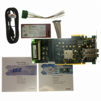
Related parts for HW-V5-ML555-G


HW-V5-ML555-G Summary of contents
Page 1
Virtex-5 FPGA ML555 Development Kit for PCI and PCI Express Designs User Guide UG201 (v1.4) March 10, 2008 R ...
Page 2
Xilinx is disclosing this Document and Intellectual Property (hereinafter “the Design”) to you for use in the development of designs to operate on, or interface with Xilinx FPGAs. Except as stated herein, none of the Design may be copied, reproduced, ...
Page 3
Date Version 02/27/07 1.2 Changed document title and updated FPGA device speed grade as "-1C ES". Updated Power,” page PCI™ Edge Connector pinout. Updated reference DDR2 reference design included with kit. Added lane assignments to Table 3-20, page circuits on ...
Page 4
Date Version 03/10/08 1.4 Added additional reference documents and application notes in Documentation,” page ML555 Development Kit,” page including removal of Virtex-5 LogiCORE Endpoint Block Wrapper. Included Platform USB Programming Cable and ISE Evaluation Software in Specified 30 MHz LVCMOS ...
Page 5
... Available Xilinx Accessories . . . . . . . . . . . . . . . . . . . . . . . . . . . . . . . . . . . . . . . . . . . . . . . 16 Conversion Module, SMA to SATA (HW-AFX-SMA-SATA) Conversion Module, SMA to RJ45 (HW-AFX-SMA-RJ45) Conversion Module, SMA to HSSDC2 (HW-AFX-SMA-HSSDC2) PHY Daughtercard (HW-AFX-BERG-EPHY) Chapter 2: Getting Started Documentation and Reference Design CD ...
Page 6
GTP Reference Clock Inputs . . . . . . . . . . . . . . . . . . . . . . . . . . . . . . . . . . . . ...
Page 7
R About This Guide This user guide is a description of the Virtex™-5 FPGA ML555 Development Kit for PCI™ and PCI Express of FPGAs is available on the Xilinx website at http://www.xilinx.com/virtex5. Guide Contents This manual contains the following chapters: ...
Page 8
Preface: About This Guide • Virtex-5 FPGA RocketIO GTP Transceiver User Guide This user guide describes the RocketIO™ GTP transceivers available in the Virtex-5 LXT and SXT platform devices. • Virtex-5 FPGA Embedded Tri-Mode Ethernet MAC User Guide This user ...
Page 9
R 12. XAPP693, A CPLD-Based Configuration and Revision Manager for Xilinx Platform Flash PROMs and FPGAs The Endpoint Block Plus for PCI Express solution from Xilinx is a reliable, high- bandwidth, scalable serial interconnect building block for use with the ...
Page 10
Preface: About This Guide Typographical Conventions This document uses the following typographical conventions. An example illustrates each convention. Convention Italic font Underlined Text 10 Meaning or Use See the Virtex-5 FPGA References to other documents Configuration Guide for more information. ...
Page 11
R Online Document The following conventions are used in this document: Convention Blue text Red text Blue, underlined text Virtex-5 FPGA ML555 Development Kit UG201 (v1.4) March 10, 2008 Typographical Conventions Meaning or Use See the section Documentation” Cross-reference link ...
Page 12
Preface: About This Guide 12 www.xilinx.com Virtex-5 FPGA ML555 Development Kit R UG201 (v1.4) March 10, 2008 ...
Page 13
... PCI Express operation. Additional information and design resources associated with the ML555 development kit is available at: http://www.xilinx.com/products/devkits/HW-V5-ML555-G.htm Parallel Bus Development for PCI Operation This Virtex-5 FPGA based kit provides a development platform for designing and verifying PCI and PCI-X™ applications utilizing Xilinx LogiCORE™ intellectual property (IP) cores ...
Page 14
Chapter 1: Introduction The ML555 board is supported by Xilinx LogiCORE IP versions 4 and 6, respectively. Each core has a primary version number, shown in number. More information about the current versions of these cores is available in the ...
Page 15
R Serial Bus Development The ML555 board is supported by a LogiCORE endpoint wrapper to configure the Integrated Endpoint Block for PCI Express operation in Virtex-5 LXT and SXT FPGAs: • Virtex-5 FPGA LogiCORE Endpoint Block Plus Wrapper for PCI ...
Page 16
... Conversion Module, SMA to SATA (HW-AFX-SMA-SATA) The SMA to SATA module can be used in conjunction with the ML555 SMA connectors. The ML555 only provides one set of SMA connectors, whereas the HW-AFX-SMA-SATA conversion module contains two sets of SMA connectors and two SATA connectors. DC power is not provided to the SATA disk drive from either the ML555 board or the conversion module ...
Page 17
... R The SMA to RJ45 conversion module can be ordered from Xilinx as part number HW-AFX- SMA-RJ45. Contact your local sales office for pricing information. Additional information on the conversion module is available from the Xilinx website at: www.xilinx.com/xlnx/xebiz/designResources/ip_product_details.jsp?key=HW-AFX-SMA-RJ45 Conversion Module, SMA to HSSDC2 (HW-AFX-SMA-HSSDC2) The SMA to HSSDC2 module can be used in conjunction with the ML555 SMA connectors to convert the SMA interface to a HSSDC2 interface ...
Page 18
Chapter 1: Introduction 18 www.xilinx.com Virtex-5 FPGA ML555 Development Kit R UG201 (v1.4) March 10, 2008 ...
Page 19
R Getting Started This chapter describes the items needed to configure the Virtex-5 FPGA ML555 board. The ML555 board is tested prior to shipment and should work out of the box. The installer is recommended to inspect the board prior ...
Page 20
Chapter 2: Getting Started 20 www.xilinx.com Virtex-5 FPGA ML555 Development Kit R UG201 (v1.4) March 10, 2008 ...
Page 21
R Hardware Description A high-level block diagram of the Virtex-5 FPGA ML555 board is shown in followed by a brief description of each board section. ML555 board with the key interfaces marked. Connector (J5) SODIMM (J2) 125 and 200 MHz ...
Page 22
Chapter 3: Hardware Description XC5VLX50T FPGA P1: Bus Connector for PCI/PCI-X Designs User Pushbuttons/LEDS The CD included in the kit contains ML555 board schematics and layout files. 22 J3: SFP1 J4: SFP2 J5: Serial ATA Figure 3-2: Annotated ML555 Board ...
Page 23
R Edge Connector for PCI Express Operation Caution! connectors. Before plugging the ML555 board into the system unit, the power configuration header settings must be reviewed to verify that the board will be powered properly. Failure to configure the power ...
Page 24
Chapter 3: Hardware Description Table 3-1 shows the connector pin assignment for PCI Express designs. The board supports x1, x4, and x8 endpoint designs. The ML555 board is an endpoint add-in card. Port names are with respect to the system ...
Page 25
R Table 3-1: P13 Edge Connector Socket Pinout for PCI Express Designs (Continued) P13 A Side A30 A31 A32 A33 A34 A35 A36 A37 A38 A39 A40 A41 A42 A43 A44 A45 A46 A47 A48 A49 Notes: 1. PCIE_PRSNT1_B can ...
Page 26
Chapter 3: Hardware Description add-in card. More than one PRSNT2_B pin is defined in the x4, x8, and x16 PCI Express connectors; these are necessary to support up-plugging of the add-in card. Up-plugging is defined as plugging a smaller link ...
Page 27
R Table 3-3: PCI Express Signals, Add-in Card Connector Pin, and FPGA Pins per GTP_DUAL Tile (1) PCI Express Signal Name PCIE_REFCLK_P PCIE_REFCLK_N PETP0 PETN0 PERP0 PERN0 PETP1 PETN1 PERP1 PERN1 PETP2 PETN2 PERP2 PERN2 PETP3 PETN3 PERP3 PERN3 PETP4 ...
Page 28
Chapter 3: Hardware Description Table 3-3: PCI Express Signals, Add-in Card Connector Pin, and FPGA Pins per GTP_DUAL Tile (1) PCI Express Signal Name PETP6 PETN6 PERP6 PERN6 PETP7 PETN7 PERP7 PERN7 PCIE_PERST Notes: 1. Signal names are with respect ...
Page 29
R 64-bit Edge Connector for PCI Operation Caution! connectors. Before plugging the ML555 board into the system unit, the power configuration header settings must be reviewed to verify that the board will be powered properly. Failure to configure the power ...
Page 30
Chapter 3: Hardware Description Table 3-4 shows the edge connector (P1) pin assignment. The component side of the PCB is side A, and the non-component side or the back of the PCB is side B. Table 3-4: P1 PCI Edge ...
Page 31
R Table 3-4: P1 PCI Edge Connector Pinout (Continued Signal FPGA Pin Side A32 EDGE_AD16 A33 VCC3V3 A34 EDGE_FRAME_B A35 GND A36 EDGE_TRDY_B A37 GND A38 EDGE_STOP_B A39 VCC3V3 A40 unused A41 unused A42 GND A43 EDGE_PAR A44 ...
Page 32
Chapter 3: Hardware Description Table 3-4: P1 PCI Edge Connector Pinout (Continued Signal FPGA Pin Side A65 EDGE_CBE5 A66 VCC3V3 A67 EDGE_PAR64 A68 EDGE_AD62 A69 GND A70 EDGE_AD60 A71 EDGE_AD58 A72 GND A73 EDGE_AD56 A74 EDGE_AD54 A75 VCC3V3 ...
Page 33
R The PCI bus on the board schematics has signal names of the form EDGE_<signal name> (denoting the card edge connector signals). The signal names listed in the A Side and B Side columns of The ML555 board supports both ...
Page 34
Chapter 3: Hardware Description provided with the cores: a simple one-doubleword (DW) register behind the I/O BAR and memory behind the memory BAR. To use the provided example implementation for PCI operation: 1. Load the bitstream onto ...
Page 35
R the DQ and DQS ports on the SODIMM side of the interface. The Xilinx Digitally Controlled Impedance (DCI) standard SSTL18_I_DCI can be utilized to terminate unidirectional address and control signals transmitted by the FPGA. External 50 Ω reference resistors ...
Page 36
Chapter 3: Hardware Description Table 3-5: SDRAM Interface Signal Descriptions (Continued) SODIMM Signal FPGA Pin Front 51 DQS2 AA29 53 GND 55 DQ18 AJ31 57 DQ19 AK31 59 GND 61 DQ24 AA25 63 DQ25 AA26 65 GND 67 DM3 AC28 ...
Page 37
R Table 3-5: SDRAM Interface Signal Descriptions (Continued) SODIMM Signal FPGA Pin Front 117 DDR2_VCC1V8 119 No connect 121 GND 123 DQ32 AB28 125 DQ33 AA28 127 GND 129 DQS4_B AK27 131 DQS4 AK28 133 GND 135 DQ34 AG28 137 ...
Page 38
Chapter 3: Hardware Description Table 3-5: SDRAM Interface Signal Descriptions (Continued) SODIMM Signal FPGA Pin Front 183 GND 185 DM7 AJ9 187 GND 189 DQ58 AM12 191 DQ59 AM11 193 GND 195 SDA AD9 197 SCL AE8 199 DDR2_VCC1V8 Notes: ...
Page 39
R Small Form-factor Pluggable (SFP) Module Interface The ML555 board has two SFP connectors that support user-installed SFP modules to support Fibre Channel and Gigabit Ethernet interfaces. The interface is compliant with the multi-source agreement specification entitled Cooperation Agreement for ...
Page 40
... SATA baud rates. A second SATA interface can be supported using the SMA connectors on the board and an external SMA to SATA interface board available from Xilinx with part number HW-AFX-SMA-SATA. The SATA and SMA transceivers are connected to a common GTP primitive block in the FPGA. ...
Page 41
... Ethernet PHY Daughtercard Support The ML555 board provides a Xilinx Generic Interface (XGI) connector system wired to support attachment of the Xilinx Ethernet PHY Daughtercard, part number HW-AFX- BERG-EPHY. The EPHY daughtercard is not included with the development kit but can be purchased separately. The XC5VLX50T FPGA has up to four embedded tri-mode Ethernet MAC blocks that provide the data link layer interface to the external PHY ...
Page 42
... GND 60 GND 62 GND 64 GND Notes: 1. UG065 [Ref 3] provides additional information on the HW-AFX-BERG-EPHY Daughtercard. 2. These signals are connected to FPGA banks 12 and 20. The bank reference voltage the CD-ROM for additional information. 3. These clocks are connected to FPGA clock-capable I/O pins connect. 42 (1) J15-ODD Signal 1 ...
Page 43
R Table 3-11: Ethernet PHY Daughtercard J16 Connection J16-EVEN Signal 2 GND 4 GND 6 GND 8 GND 10 GND 12 GND 14 GND 16 GND 18 GND 20 GND 22 GND 24 GND 26 GND 28 GND 30 GND ...
Page 44
... The LVDS transmit and receive connectors can be connected to each other for loopback testing as shown in with the kit, but can be ordered separately from Xilinx as part number HW-LVDS-CBL-80. The LVDS transmit and receive connectors can also be connected to either an ML450 or ML550 networking interfaces board from Xilinx. Additional information on Xilinx board products is located at www ...
Page 45
R Table 3-12 Table 3-12: SAMTEC Pin Connections (P32) SAMTEC-QSE- 028-DP P32 Odd Virtex-5 FPGA ML555 Development Kit UG201 (v1.4) March 10, 2008 Figure 3-5: LVDS and Mezzanine Card Connectors and Table 3-13 list the SAMTEC ...
Page 46
Chapter 3: Hardware Description Table 3-12: SAMTEC Pin Connections (P32) (Continued) SAMTEC-QSE- 028-DP P32 Odd ...
Page 47
R Table 3-12: SAMTEC Pin Connections (P32) (Continued) SAMTEC-QSE- 028-DP P32 Odd Notes: 1. These signals are connected to FPGA banks 1 and 19. The FPGA reference voltage for these banks is 2.5V. See the ML555 ...
Page 48
Chapter 3: Hardware Description Table 3-13: SAMTEC Pin Connections (P33) (Continued) SAMTEC-QSE- 028-DP P33 Odd Notes: 1. These signals ...
Page 49
R SAMTEC QSE-028-DP J12 80 H12 K24 68 L24 J24 J25 J27 J26 54 52 H25 50 H24 G27 H27 42 E28 40 F28 ...
Page 50
Chapter 3: Hardware Description SAMTEC Mezzanine Expansion Card Support The ML555 board supports the addition of mezzanine boards attached to connectors P32 and P33 power is provided to the mezzanine board on connector P48 (see Table 3-14). A ...
Page 51
R Table 3-16: RS-232 Interface Signal Names and Pin Assignments (Continued) Signal Name FPGA In/Out USB_RST_B In/Out USB_SUSPEND_B In Notes: 1. These signals are connected to FPGA bank 1. The FPGA reference voltage, V schematics on the CD-ROM for additional ...
Page 52
Chapter 3: Hardware Description be configured as a serial COM port for the user to continue working with serial communication utilities like HyperTerminal or Tera Term Pro. The CP210x USB-to-UART Bridge VCP drivers can be downloaded from the Silicon Laboratories ...
Page 53
R Table 3-18 regional clock input and a global clock input of the FPGA as shown in differential 100 MHz reference clock input for PCI Express designs (PCIE_REFCLK{P/N}) is described in (PCI Express Operation),” page inputs as well as global ...
Page 54
Chapter 3: Hardware Description Table 3-18: ML555 Board Clock Sources (Continued) Clock Designator Output PCIE_REFCLKN Differential (system board input) Notes: 1. Differential clock inputs to the FPGA should use the IBUFDS input buffer library primitive. Setting the DIFF_TERM attribute of ...
Page 55
R Figure 3-8 shows a block diagram of the default clock synthesis configuration, provided on production ML555 boards. FPGA_GCLK_30MHZ SMA_GCLKP J10 SMA_GCLKN J11 P13-A13 PCIE_REFCLK P13-A14 Clock 0 Synth 10 MHz #1 1 Clock 0 25 MHz Synth #2 1 ...
Page 56
Chapter 3: Hardware Description Figure 3-9 attenuator circuit. Contact your local Xilinx representative for more information on this option. FPGA_GCLK_30MHZ SMA_GCLKP J10 SMA_GCLKN J11 P13-A13 PCIE_REFCLK P13-A14 874003 Clock 0 Synth 10 MHz 1 #1 Clock 0 25 MHz Synth ...
Page 57
R Global Clock Inputs Global clock inputs to the FPGA are summarized in connected to FPGA bank 3. Table 3-19: FPGA Global Clock Inputs FPGA Pins Signal Name L18 LVPECL_200M_N K17 LVPECL_200M_P H18 SMA_GCLKN (2,5) H17 SMA_GCLKP (2,5) H19 LVDSCLKMOD1_P ...
Page 58
Chapter 3: Hardware Description Table 3-19: FPGA Global Clock Inputs (Continued) FPGA Pins Signal Name K18, K19, H13 No connects Notes coupled. 2. The SMA clock input can be differential or single ended. When driven with a single ...
Page 59
R PCI Express applications can utilize the system board’s 100 MHz clock input on the GTP MGTREFCLK clock input or synthesize a 100 MHz clock using the clock synthesizer, a DCM, and GTP clocking resources. SATA applications must synthesize a ...
Page 60
Chapter 3: Hardware Description Serial Bus Clocking with Optional ICS874003-02 Clock Jitter Attenuator (PCI Express Operation) By default, the ML555 board connects the PCIE_REFCLK input from the add-in card connector, through two DC blocking capacitors, and then to GTP X0Y2 ...
Page 61
R Clock Synthesizers The ML555 board contains two clock synthesizer circuits that support a wide range of frequency synthesis capabilities for end-user applications. One of the clock synthesizers should be used to generate the clock for the DDR2 SODIMM memory. ...
Page 62
Chapter 3: Hardware Description Table 3-21: ICS8442 Divisor Switch Settings SW12-9 or SW12-10 “N1” Notes logic “0” is obtained by moving the switch to the “OPEN” position, and a logic “1” is obtained by ...
Page 63
R SW10: Parallel Load Inputs for ICS1 SW9: Parallel Load ICS1 Pushbutton switch SW9 is used to parallel-load the multiplier and divisor selections for Synthesizer 1 (U8), and switch SW11 is used to parallel-load the multiplier and divisor DIP switch ...
Page 64
Chapter 3: Hardware Description output clock is not deterministic. Only one output frequency can be generated based upon the divisor selection. Table 3-22: Clock Synthesizer 1 Frequency Output for Multiplier/Divider Values with a 10 MHz Input Clock Multiplier Input Selection ...
Page 65
R Table 3-22: Clock Synthesizer 1 Frequency Output for Multiplier/Divider Values with a 10 MHz Input Clock (Continued) Multiplier Input Selection (hex) VCO Lock Frequency Range (MHz) M8 M[7: 530 0 36 540 0 37 550 0 38 ...
Page 66
Chapter 3: Hardware Description Table 3-23 M and divisor N inputs to the ICS8442 device with a 25 MHz reference clock input for Clock Synthesizer 2. Table 3-23: Clock Synthesizer 2 Frequency Output for Multiplier/Divider Values with a 25 MHz ...
Page 67
R Table 3-24 the switch positions assigned for the M and N constants. When the switch is in the ON position, a logic “1” is obtained, and in the OFF position, a logic “0” is obtained. Figure 3-12 positions are ...
Page 68
Chapter 3: Hardware Description Logic 0 Position Example requests ICS1 330 MHz Clock with M(8:0) = 0x021 and N(1: Serial Mode Operation The FPGA provides interface signals to program each synthesizer in serial mode. Table ...
Page 69
R Table 3-25: FPGA Signals for Serial Programming of the Clock Synthesizer Modules (Continued) Signal LVDSCLKMOD1_P Clock Synthesizer 1 clock outputs. See representation of the clock network on the ML555 board. LVDSCLOCKMOD1_N MGT_X0Y1_RCLKP MGT_X0Y1_RCLKN PLOAD_2 ICS8442 parallel load input used ...
Page 70
Chapter 3: Hardware Description Figure 3-13 operation. The parallel mode has priority over serial mode. SCLOCK SDATA T1 T0 NULL STROBE M,N PLOAD Figure 3-13: Serial Configuration Interface Timing Clock-Capable I/O Pins Associated with Clock Inputs Some clock-capable input and ...
Page 71
... User-defined LVDS general-purpose I/O 1 2.5 interface User-defined LVDS general-purpose I/O 2 2.5 interface Ethernet PHY clocks from daughtercard 12 2.5 HW-AFX-BERG-EPHY 20 2.5 Ethernet PHY clocks from daughtercard HW-AFX-BERG-EPHY User defined Potential dynamic reconfiguration request or other user-defined application using a core for PCI operation www.xilinx.com Clock Generation Function 71 ...
Page 72
Chapter 3: Hardware Description Table 3-26: FPGA Clock-Capable I/O Connectivity (Continued) Signal Name FPGA Pin FPGA Bank Bank V DQS2_B AA30 DQS2 AA29 DQS1_B AC30 DQS1 AB30 DQS0_B AA31 DQS0 AB31 DQS5_B AJ26 DQS5 AH27 DQS4_B AK27 DQS4 AK28 DQS3_B ...
Page 73
R 3. Using one of the clock synthesizer chips. If using the parallel input mode, SW9 and/or SW11 must be pressed and released to obtain a known output frequency from the clock synthesizers after a power-on cycle. ♦ Typically, CLOCK_SYNTH1 ...
Page 74
Chapter 3: Hardware Description User Pushbutton Switches The ML555 board provides three user pushbutton switches. The switch outputs are pulled up to 2.5V using 4.7 KΩ resistors on the board. The pushbuttons generate a switch closure to GND when pressed. ...
Page 75
R Voltage Regulators The ML555 board is powered from either the PCI slot that it is plugged into, utilizing the +5V and the +3.3V power rails (see edge connector pinout), or the PCI Express slot that it is plugged into ...
Page 76
Chapter 3: Hardware Description 3.3V System Motherboard Slot/Connector PCI Bus Sources 3.3V and 5V and PCI Express Sources 3.3V and 12V Caution! system unit. Failure to configure the board jumpers prior to installation in the system unit might cause damage ...
Page 77
R Figure 3-15 jumper MUST be configured prior to installing the board in the system unit. SW8 selects the FPGA V for PCI Express operation. SW8: FPGA V Source Selection CCINT Parallel PCI Bus Mode: Switch Position “1” towards PCI ...
Page 78
Chapter 3: Hardware Description Figure 3-16 PCI-X Bus power configurations. Serial PCI Express Power Configuration 2 1 P18 4 3 Slide Switch PCIe PCI SW8 ML555 Board SODIMM Before installing the ML555 board in a system unit, the power system ...
Page 79
R The SW8 switch (the source of the 3V power) must be configured according to to generate GTP transceiver analog and FPGA V Table 3-31: V Voltage Source Selection for PCI or PCI Express Bus Applications CCINT 3.3V Power to ...
Page 80
Chapter 3: Hardware Description Add-in Card DC Power Input (PCI Express Operation) For PCI Express applications, the ML555 board has +3.3V and +12V power available from the system unit power supply. The ML555 board does not use the 3.3V AUX ...
Page 81
R Table 3-34: ML555 Onboard DC-to-DC Voltage Converters Input Voltage Source ML555 Board Reference (1) Designator PCI or PCI-X Mode (4) (2) VR1 Not Used (5) VR2 PCI Connector 5V Input (5) VR3 PCI Connector 5V Input (5) U12 PCI ...
Page 82
Chapter 3: Hardware Description GTP Transceiver Power Three low drop-out (LDO) voltage regulators are provided for the analog voltage inputs to the GTP transceivers. Each regulator has a voltage divider circuit that permits the voltage to be adjusted, if required, ...
Page 83
The ML555 board provides headers that can be used to monitor the three GTP transceiver analog power supplies as well as the internal FPGA voltage V applications, power sensing is provided on the output of the +12V ...
Page 84
Chapter 3: Hardware Description Table 3-36: ML555 Voltage Sensing Power Measurement Headers Voltage Name AVTTX AVCCPLL AVCC V CCINT 12V-to-5V Converter for PCI Express Applications 84 P44 Figure 3-18: Power Measurement Headers Description 1.2V GTP Analog Termination Voltage 1.2V GTP ...
Page 85
R The ML555 board cannot margin any of the oncard power supplies. Other Xilinx boards have power supply monitoring and margining capabilities for application-specific functions, such as memory interfaces and LVDS interfaces. Characterization boards are available for GTP transceiver characterization. ...
Page 86
Chapter 3: Hardware Description XCF32PFS48C Platform Flash U1 and U15 Figure 4-5, page 92 the XC5VLX50T FPGA U10 and the XC2C32 CPLD U6. The XCF32PFS48C V The Platform Flash holds up to four configuration images for the XC5VLX50T FPGA, two ...
Page 87
R Configuration The Virtex-5 FPGA ML555 board includes several options to configure the XC5VLX50T FPGA, XC2C32 CoolRunner-II CPLD, and the XCF32PF Platform Flash. The basic configuration modes for the Virtex-5 family are: • JTAG mode via Parallel Cable IV, Platform ...
Page 88
Chapter 4: Configuration U10: FPGA SW5: Mode Switch SW6:PROG P3 88 U6: CPLD P39 P2 Figure 4-1: Configurable Devices www.xilinx.com SW7: RST U1: Platform Flash P38 P5: JTAG Connector P20 UG201_c4_01_091806 Virtex-5 FPGA ML555 Development Kit UG201 (v1.4) March 10, ...
Page 89
R Configuration Modes Table 4-1 shows the Virtex-5 FPGA configuration modes along with the correct settings for the Configuration Mode switch (SW5). Table 4-1: Configuration Modes Master SelectMAP Slave SelectMAP JTAG Master Serial Slave Serial Notes: 1. Switch position 4 ...
Page 90
Chapter 4: Configuration connector/header P38 is used to enable or bypass the Platform Flash device U1, and connector/header P20 is used to enable or bypass the second Platform Flash device U15. To enable the CPLD for JTAG configuration, the shunts ...
Page 91
R Table 4-2: P5 JTAG Header Signal Descriptions and Pin Assignments Signal Name JTAG_TMS JTAG_TCK JTAG_TDO JTAG_TDI Notes: 1. This JTAG connectivity assumes that all four devices are in the JTAG configuration chain. 2. The JTAG_TDO connection is made to ...
Page 92
Chapter 4: Configuration U15 U1 Platform Flash Platform Flash XCF32PF XCF32PF D[0:7] CE1 (U15) CE (U1) BUSY OE/RESET CLKOUT To P2 REV_SEL0 CLKIN From P2 REV_SEL1 Notes: 1. FORCE, WIDE, PCIW_EN, and RTR are FPGA general-purpose ...
Page 93
R Table 4-3: FPGA Configuration Pin Listing Pin Net Name Direction Number M15 FPGA_DONE AD15 FPGA_BUSY_B (5) AD19, FLASH_D0 P15 (5) AE19 FLASH_D1 (5) AE17 FLASH_D2 (5) AF16 FLASH_D3 (5) AD20 FLASH_D4 (5) AE21 FLASH_D5 (5) AE16 FLASH_D6 (5) AF15 ...
Page 94
Chapter 4: Configuration Table 4-4: CPLD Pin Listing Pin Net Name Number 1 CPLD_CLK_30MHZ 2 FLASH_IMAGE0_SELECT 3 FLASH_IMAGE1_SELECT 4 GND 5 FPGA_DONE 6 FPGA_BUSY_B 7 VCC2V5 8 PROG_SW_B 9 FPGA_TDO 10 JTAG_TMS 11 JTAG_TCK 12 ICS_FSEL2 13 MAN_AUTO_B 14 ICS_MR ...
Page 95
R Table 4-4: CPLD Pin Listing (Continued) Pin Net Name Number (1) 32 RTR (1) 33 PCIW_EN 34 FPGA_RDWR_B 35 VCC2V5 36 CPLD_SPARE3 37 PCIE_RST 38 FLASH_CE1_B 39 FLASH_REV_SEL0 40 FLASH_REV_SEL1 41 BUSY_TO_FLASH_B 42 FLASH_CE_B 43 FLASH_CF_B 44 FLASH_OE_RESET_B Notes: ...
Page 96
Chapter 4: Configuration Table 4-5: Pin Listing for Platform Flash (Continued) Pin Net Name Number H5 FLASH_D1 E5 FLASH_D2 D5 FLASH_D3 C5 FLASH_D4 B5 FLASH_D5 A5 FLASH_D6 A6 FLASH_D7 H4 FLASH_EN_EXT_SEL_B A3 FLASH_OE_RESET_B G3 FLASH_REV_SEL0 G4 FLASH_REV_SEL1 H3 JTAG_TCK E6 ...
Page 97
R Table 4-5: Pin Listing for Platform Flash (Continued) Pin Net Name Number D2 Unused D3 Unused D4 Unused E3 Unused E4 Unused F2 Unused F3 Unused F4 Unused G2 Unused Notes: 1. The ML555 board uses 2.5V I/O drivers ...
Page 98
Chapter 4: Configuration U15 Platform Flash U1 XCF32PF Platform Flash D[0:7] XCF32PF CE1 (U15) CE (U1) BUSY OE/RESET To P2 CLKOUT REV_SEL0 CLKIN From P2 REV_SEL1 Notes: 1. FORCE, WIDE, PCIW_EN, and RTR are FPGA general-purpose I/Os. ...
Page 99
R simply specifies the bitstream revision along with a signal to indicate when to start the configuration process. Logic within the CPLD then controls the configuration pins to the FPGA and Platform Flash to complete the configuration cycle. This logic ...
Page 100
Chapter 4: Configuration SelectMAP Clock Selection The default configuration of the ML555 board is to provide Master SelectMAP configuration with the FPGA providing the configuration clock (CCLK) to both the FPGA and Platform Flash devices. Slave SelectMAP configuration is not ...
Page 101
R Platform Flash Image Generation and Programming This section provides general guidelines on how to create a PROM image file with two design revisions (bitstreams) using the Configuration File Wizard in the iMPACT FPGA programming tool. Online documentation from the ...
Page 102
Chapter 4: Configuration 3. Under Prepare PROM Files, shown in ♦ Under I want to target a, click the PROM Supporting Multiple Design Versions radio button and select XCFP PROM with Design Revisioning from the drop-down menu. ♦ Under PROM ...
Page 103
R Specifying the Xilinx PROM Device Follow these steps to specify the PROM device: 1. Under Specify Xilinx PROM Device, shown in ♦ From the Number of Revisions drop-down box, choose 2. The XCF32P supports a maximum of two XC5VLX50T ...
Page 104
Chapter 4: Configuration Under Generate PROM File → Do you want to compress file?, click No. 9. 10. After a pause, PROM File Generation Succeeded is displayed. A PROM image file is now created and is ready for programming into ...
Page 105
R Figure 4-12: ML555 JTAG Chain with All Four Programmable Devices in the Chain Virtex-5 FPGA ML555 Development Kit UG201 (v1.4) March 10, 2008 Platform Flash Image Generation and Programming Figure 4-11: Initialize JTAG Chain with iMPACT Tool www.xilinx.com UG201_c4_14_052307 ...
Page 106
Chapter 4: Configuration 106 Figure 4-13: Programming Properties Figure 4-14: Advanced PROM Programming Properties www.xilinx.com UG201_c4_11_052307 UG201_c4_12_022007 Virtex-5 FPGA ML555 Development Kit UG201 (v1.4) March 10, 2008 R ...
Page 107
R Virtex-5 FPGA ML555 Development Kit UG201 (v1.4) March 10, 2008 Platform Flash Image Generation and Programming Figure 4-15: PROM Revision Properties www.xilinx.com UG201_c4_13_022007 107 ...
Page 108
Chapter 4: Configuration 108 www.xilinx.com Virtex-5 FPGA ML555 Development Kit R UG201 (v1.4) March 10, 2008 ...