R0K564112S000BE#WS Renesas Electronics America, R0K564112S000BE#WS Datasheet
R0K564112S000BE#WS
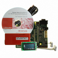
Specifications of R0K564112S000BE#WS


Related parts for R0K564112S000BE#WS


R0K564112S000BE#WS Summary of contents
Page 1
To our customers, Old Company Name in Catalogs and Other Documents st On April 1 , 2010, NEC Electronics Corporation merged with Renesas Technology Corporation, and Renesas Electronics Corporation took over all the business of both companies. Therefore, although the ...
Page 2
All information included in this document is current as of the date this document is issued. Such information, however, is subject to change without any prior notice. Before purchasing or using any Renesas Electronics products listed herein, please confirm ...
Page 3
Renesas Starter Kit for R32C/111 User’s Manual RENESAS SINGLE-CHIP MICROCOMPUTER R32C/100 Series WS TOOL Rev.0.90 2008.11 ...
Page 4
By using this Renesas Starter Kit (RSK), the user accepts the following terms. The RSK is not guaranteed to be error free, and the entire risk as to the results and performance of the RSK is assumed by the User. ...
Page 5
Table of Contents Chapter 1. Preface .................................................................................................................................................. 1 Chapter 2. Purpose ................................................................................................................................................. 2 Chapter 3. Power Supply ........................................................................................................................................ 3 3.1. Requirements ............................................................................................................................................... 3 3.2. Power–up Behaviour .................................................................................................................................... 3 Chapter 4. Board Layout ......................................................................................................................................... 4 4.1. Component Layout ....................................................................................................................................... 4 4.2. ...
Page 6
Cautions This document may be, wholly or partially, subject to change without notice. All rights reserved. No one is permitted to reproduce or duplicate, in any form, a part or this entire document without the written permission of Renesas Technology ...
Page 7
This RSK is an evaluation tool for Renesas microcontrollers. Features include: • Renesas Microcontroller Programming. • User Code Debugging. • User Circuitry such as switches, LEDs and potentiometer(s). • Sample Application. • Sample peripheral device initialisation code. The RSK board ...
Page 8
Chapter 3. Power Supply 3.1. Requirements This RSK board operates from power supply (supplied). A diode provides reverse polarity protection only if a current limiting power supply is used. All RSK boards are supplied with an E8A ...
Page 9
Component Layout The following diagram shows the top layer component layout of the board. Chapter 4. Board Layout Figure 4-1: Board Layout 4 ...
Page 10
Board Dimensions 5 ...
Page 11
Chapter 5. Block Diagram Figure 5-1 shows the RSK board components and their connectivity. Figure 5-2 shows the E8A connections to the RSK. Host PC Figure 5-1: Block Diagram USB Cable E8A Module Pin 1 E8A MCU E30A CPU Board ...
Page 12
Switches There are four switches located on the RSK board. The function of each switch and its connection are shown in Table 6-1: Switch Functions Switch RES When pressed, the microcontroller is reset. SW1 / BOOT* Connects to an ...
Page 13
Description Function UART0 Default serial port (TX) UART0 Default serial port (RX) UART1 Spare Serial Port (TX) UART1 Spare Serial Port (RX) The board is designed to accept a straight-through RS-232 male-to-female cable. The second transceiver channels are connected to ...
Page 14
Reference Function R23 Serial Port Disables the RS-232 Transceiver. Configuration (Must be removed if R27 is fitted.) Enables the RS-232 Transceiver. R27 Serial Port Configuration (Must be removed if R23 is fitted.) R28 Serial Port Connects the programming port (Rx) ...
Page 15
Reference Function R30 E8A Connects the serial programming Configuration port (Rx) to the E8A connector R36 E8A Connects the serial programming Configuration port (Tx) to the E8A connector Connects the serial programming R40 E8A Configuration port (CK) to the E8A ...
Page 16
Reference Function R13 Power Source Board can be powered from the PWR connector. R22 Power source Connects Board_VCC2 to PWR supply. R24 Microcontroller Supply power to the Microcontroller Power Supply pin VCC2. R25 Power source Connect Board_VCC2 to CON_3V3. Connect ...
Page 17
Reference Function R49 Application Board Connects MCU port pin p2_4 (pin 66) to Interface DLCDD4 on Debug LCD Header R50 Application Board Connects MCU port pin p2_6 (pin 64) to Interface DLCDD6 on Debug LCD Header R51 Application Board Connects ...
Page 18
R75 Application Board Connects MCU port pin p2_5 (pin 65) to Interface DLCDD5 on Debug LCD Header R76 Application Board Connects MCU port pin p2_7 (pin 63) to Interface DLCDD7 on Debug LCD Header R77 Application Board Connects MCU port ...
Page 19
R99 Application Board Connects MCU port pin p7_4 (pin 24) to Interface Wp at JA2-17 R101 Application Board Connects MCU port pin p7_4 (pin 24) to Interface TA2OUT at JA2-19 R102 Application Board Connects MCU port pin p7_5 (pin 23) ...
Page 20
R135 Application Board Connects MCU port pin p10_7 (pin 87) Interface to CAN1_STBn Table 6-10 below describes the function of the option links associated with Clock configuration. Reference Function R120 Main clock Connects the external clock to the MCU. R124 ...
Page 21
The reset circuit operates by latching the state of the boot switch (SW1) on pressing the reset button. This control is subsequently used to modify a port pin state to select which code is executed. The reset is held in ...
Page 22
The MCU can be configured in User mode and Boot mode. User mode may be used to run and debug user code, while Boot mode may only be used to program the MCU with program code via the serial interface. ...
Page 23
Chapter 8. Programming Methods The board is intended for use with HEW and the supplied E8A debugger only. Please refer to R32C/111 Group Hardware Manual for details of the programming methods using the on-chip serial port and without using E8A ...
Page 24
Microcontroller Ring Headers The microcontroller pin headers and their corresponding microcontroller connections are detailed in Table 9-1 to Table 9-4. Pin Circuit Net Name 1 CAN1_OUT 3 DA1 5 P9_2 7 P9_0 9 P14_5 11 P14_3 13 P14_1 15 ...
Page 25
Pin Circuit Net Name 1 IIC_SDA_TxD2 3 UC_VCC1 5 GROUND 7 E8_BUSY 9 RxD0 11 CTSRTS 13 P13_6 15 P13_4 17 ALE GROUND 23 UC_VCC1 25 P13_0 27 RDn 29 WRLn_WRn 31 P12_6 33 A23_CS0n 35 A21_CS2n ...
Page 26
Pin Circuit Net Name 1 A19_LED3 3 A18_LED2 5 A17_LED1 7 A15_IO7 9 A13_IO5 11 A11_IO3 13 A9_IO1 15 P12_3 17 P12_1 19 UC_VCC2 21 GROUND 23 A6_DLCDD6 25 A4_DLCDD4 A0_DLCDRS 31 D14_CAN0_ERR 33 D12 35 D10 ...
Page 27
Pin Circuit Net Name P11_3 9 P11_1 P15_7 17 P15_5 19 P15_3 21 P15_1 23 P15_0 25 AN7_CAN1_STBn 27 AN5_CAN0_STBn 29 AN3 31 AN1 33 ADPOT_AN0 35 CON_AVCC ...
Page 28
Application Headers Standard application header connections are detailed in Table 9-5 to Table 9-9. Pin Generic Header RSK board Signal Name Name 1 5V CON_5V 3 3V3 CON_3V3 5 AVcc CON_AVCC 7 AVref CON_VREF 9 AD0 11 AD2 13 ...
Page 29
Pin Generic Header RSK board Signal Name Name 1 A0 A0_DLCDRS A4_DLCDD4 7 A6 A6_DLCDD6 9 A8 A8_IO0 11 A10 A10_IO2 13 A12 A12_IO4 15 A14 A14_IO6 ...
Page 30
Pin Generic Header RSK board Signal Name Name 1 AD4 AN4 3 AD6 AN6 5 CAN1TX CAN0_OUT 7 CAN2TX CAN1_OUT 9 AD8 NC 11 AD10 NC 13 TIOC0A NC 15 TIOC0C NC 17 TCLKC NC 19 M2_Up NC 21 M2_Vp ...
Page 31
Chapter 10. Code Development 10.1. Overview Note: For all code debugging using Renesas software tools, the RSK board must either be connected serial port via a serial cable USB port via an E8A. Due ...
Page 32
Memory Map The memory map shown below gives the locations of each memory area. For more details please refer to the R32C/111 Hardware manual. Figure 10-1: Memory Map 27 ...
Page 33
Figure 10-2: Flash memory map 28 ...
Page 34
Chapter 11. Component Placement 29 ...
Page 35
Chapter 12. Additional Information For details on how to use High-performance Embedded Workshop (HEW), refer to the HEW manual available on the CD or installed in the Manual Navigator. For information about the R32C/111 microcontrollers refer to the R32C/111 Group ...
Page 36
Renesas Starter Kit for R32C/111 User's Manual Publication Date Rev.0.90 28.Nov.2008 Published by: Renesas Technology Europe Ltd. Duke’s Meadow, Millboard Road, Bourne End Buckinghamshire SL8 5FH, United Kingdom ©2008 Renesas Technology Europe and Renesas Solutions Corp., All Rights Reserved. ...
Page 37
Renesas Starter Kit for R32C/111 1753, Shimonumabe, Nakahara-ku, Kawasaki-shi, Kanagawa 211-8668 Japan User’s Manual REG10J0150-0090 ...