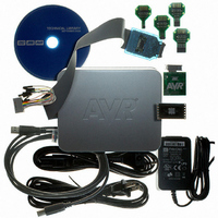
ATAVRONEKIT Atmel, ATAVRONEKIT Datasheet - Page 10

ATAVRONEKIT
Manufacturer Part Number
ATAVRONEKIT
Description
KIT AVR/AVR32 DEBUGGER/PROGRMMR
Manufacturer
Atmel
Series
AVR®r
Type
Debuggerr
Specifications of ATAVRONEKIT
Contents
Programmer/Debugger
Processor To Be Evaluated
AVR32
Data Bus Width
32 bit
Interface Type
ISP, JTAG
Core Architecture
AVR
Kit Contents
ATAVRONEKIT
Tool / Board Applications
General Purpose MCU, MPU, DSP, DSC
Development Tool Type
Hardware / Software - Dev Kit (Dev Tool)
Rohs Compliant
Yes
Mcu Supported Families
AVR32 32-bit MCU
For Use With/related Products
AVR® Devices
Lead Free Status / RoHS Status
Lead free / RoHS Compliant
Available stocks
Company
Part Number
Manufacturer
Quantity
Price
Company:
Part Number:
ATAVRONEKIT
Manufacturer:
Atmel
Quantity:
135
7. Memories
7.1
7.2
8067M–AVR–09/10
Features
Overview
•
•
•
•
The AVR architecture has two main memory spaces, the Program Memory and the Data Mem-
ory. In addition, the XMEGA A1 features an EEPROM Memory for non-volatile data storage. All
three memory spaces are linear and require no paging. The available memory size configura-
tions are shown in
memory signature row for calibration data, device identification, serial number etc.
Non-volatile memory spaces can be locked for further write or read/write operations. This pre-
vents unrestricted access to the application software.
Flash Program Memory
Data Memory
Production Signature Row Memory for factory programmed data
User Signature Row
– One linear address space
– In-System Programmable
– Self-Programming and Bootloader support
– Application Section for application code
– Application Table Section for application code or data storage
– Boot Section for application code or bootloader code
– Separate lock bits and protection for all sections
– Built in fast CRC check of a selectable flash program memory section
– One linear address space
– Single cycle access from CPU
– SRAM
– EEPROM
– I/O Memory
– External Memory support
– Bus arbitration
– Separate buses for SRAM, EEPROM, I/O Memory and External Memory access
Byte and page accessible
Optional memory mapping for direct load and store
Configuration and Status registers for all peripherals and modules
16 bit-accessible General Purpose Register for global variables or flags
SRAM
SDRAM
Memory mapped external hardware
Safe and deterministic handling of CPU and DMA Controller priority
Simultaneous bus access for CPU and DMA Controller
Device ID for each microcontroller device type
Serial number for each device
Oscillator calibration bytes
ADC, DAC and temperature sensor calibration data
One flash page in size
Can be read and written from software
Content is kept after chip erase
“Ordering Information” on page
2. In addition each device has a Flash
XMEGA A1
10


