ATAVRSB100 Atmel, ATAVRSB100 Datasheet
ATAVRSB100
Specifications of ATAVRSB100


Related parts for ATAVRSB100


ATAVRSB100 Summary of contents
Page 1
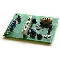
... Low-power modes • Internal temperature sensor 1 Introduction This document describes the ATAVRSB100 (SB100) smart battery development board. The SB100 is designed for evaluation of the Atmel AVR ATmega406, which is designed for smart battery applications. The ATmega406 is designed for battery packs with Li-Ion cells in series. ...
Page 2
... To use the SB100 it needs to be connected to an SMBus host/charger, a battery pack (or a simulated battery pack) and a number of jumpers need to be configured correctly. Further, for programming and debugging it is required to hook up an Atmel JTAGICE mkII. Note that ATmega406 does not support in-system serial programming ...
Page 3
... HDR2 provides access to the JTAG interface of the ATmega406, which is used for programming and debugging using the JTAGICE mkII. The use of JTAGICE mkII is described in the AVR Studio® online Users Guide and on the Atmel web. Note that the older JTAGICE does not work with this board. ...
Page 4
Cell connector (CONN2) and current sense source (JB4) 2.1.3 Wiring for battery cell simulation AVR454 4 CONN2 is used for connecting the battery cells in addition to power supply for the charge/discharge current and cell voltage simulators. Refer to ...
Page 5
Wiring for live Li-Ion battery cells 2598C-AVR-06/06 Figure 2-3. CONN2 wiring and jumper settings for battery simulation CONN2 - 24V + ±5V Table 2-4. JB3: Cell voltage simulation jumper block Pin Name Direction 1 SIM-CELL4+ 2 CELL4+ 3 SIM-CELL3+ ...
Page 6
Host/charger SMBus Connector (CONN1) AVR454 6 by changing the jumping on JB4 to pins 3-5 and 4- not necessary to rewire the CELL1- terminal to bypass the sense resistor, but this can be done if desired. Figure ...
Page 7
Safety Signal 2.1.5.2 Charger Active Signal (BATT) 2.1.6 Test Points 2598C-AVR-06/06 Table 2-5. CONN1: Battery Pack Connections to Host or Charger Pin Name Direction 1 B+ I/O 2 BATT Input 3 B- I/O 4 SAFETY Output 5 SMBCLK I/O ...
Page 8
Using the simulator stages 2.2.1 Calibrating the Cell Simulator AVR454 8 Table 2-6. Test points on SB100 Test Point Name Description TP1 Test Point 1 is the junction between the two primary power MOSFET devices, Q3 and Q4, and ...
Page 9
Simulating Charging and Discharging 2.2.3 Simulating Cell Imbalance 2.2.4 Current Simulation 2598C-AVR-06/06 When working on packs that use either a 2-cell or a 3-cell stack, the potentiometers for cells 3 and 4 (or just cell4) should be adjusted to ...
Page 10
Smart battery Circuit 2.3.1 Charging and discharging control 2.3.2 Precharge 2.3.3 Charge and discharge AVR454 10 The ATmega406 provides a highly integrated solution that makes it easy to create an SMBus compliant smart battery device with pack capacity monitoring ...
Page 11
... The PI and NI pins are the input to the Coulomb Counter ADC. Since this is a very high sensitivity input, care has been taken in the layout to ensure that leakage from other voltage sources is minimized. The layout of the ATAVRSB100 board includes GND traces, which act as leakage absorbers highly recommended to not use No-Clean flux when manufacturing production boards, as such leaves a residue that may be conductive ...
Page 12
... VR5 can now be used to adjust the voltage on all cells simultaneously. To configure the ATAVRSB100 for cell voltage simulation, all five jumpers of J3 must be installed. This ties the outputs of the buffered voltage divider stages to the cell inputs. Additionally an external power supply must be connected to CONN2 pin 1 (GND) and CONN2 pin 2 (positive) ...
Page 13
... This is jumpable directly on JB2 pins 3 and 4. Any other line that supports the Pin-Change functionality could also be used. As supplied from the factory, the ATAVRSB100 Development Kit is set up for simulation of both cell voltages and pack current. The jumpers come configured as shown in Table 2-7. ...
Page 14
... Output JB2 provides access to several I/O signals as well as extra signals used in the software implementation provided by Atmel (specifically the SMBCLK signal and the SPARE pushbutton). Additionally, power for the LEDs can be selected here to come either directly from 3.3V or from PB6 (OC0A PWM output). ...
Page 15
Thus better to use lower resistance thermistors to reduce errors. Figure 2-7 shows how to connect external thermistors to HDR1. Since the input impedance of the VADC will affect the reading, PA0 is used both for normal ...
Page 16
Appendix – Additional hardware documentation Figure 3-1. Schematic AVR454 16 2598C-AVR-06/06 ...
Page 17
Figure 3-2. Assembly drawing 2598C-AVR-06/06 AVR454 17 ...
Page 18
... XTAL, 32KHz, SMD, FC145 pkg DUAL-ROW 5x2 HEADER, 0.1" CENTER DUAL-ROW 3x2 HEADER, 0.1" CENTER 2-PIN 0.100" HEADER 0.100" SHORTING JUMPER PUSHBUTTON, SMT, BROWN OR BLACK PUSHBUTTON, SMT, RED, LM 5.00/6/90 5.0MM SCREW TERMINAL, 90' STACKABLE PCB-ATAVRSB100-D Alternate Source: # CSR1TTER005D Footprint 0603 0402 0402 0402 0402 0402 ...
Page 19
Table of Contents 2598C-AVR-06/06 Features ............................................................................................... 1 1 Introduction ...................................................................................... 1 2 The SB100 Hardware ....................................................................... 2 2.1 Connecting the SB100 ........................................................................................ 2 2.1.1 Programming and debugging (HDR2) ....................................................................... 3 2.1.2 Cell connector (CONN2) and current sense source (JB4)......................................... ...
Page 20
... ADVISED OF THE POSSIBILITY OF SUCH DAMAGES. Atmel makes no representations or warranties with respect to the accuracy or completeness of the contents of this document and reserves the right to make changes to specifications and product descriptions at any time without notice. Atmel does not make any commitment to update the information contained herein. Unless specifically provided otherwise, Atmel products are not suitable for, and shall not be used in, automotive applications. Atmel’ ...