ATAVRSB100 Atmel, ATAVRSB100 Datasheet - Page 12
ATAVRSB100
Manufacturer Part Number
ATAVRSB100
Description
SMART BATTERY DEVELOPMENT KIT
Manufacturer
Atmel
Type
Smart Batteryr
Datasheet
1.ATAVRSB100.pdf
(20 pages)
Specifications of ATAVRSB100
Contents
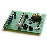
Fully Assembled Evaluation Board
Processor
ATmega406
Processor To Be Evaluated
ATmega406
Data Bus Width
8 bit
Interface Type
JTAG
For Use With/related Products
ATmega406
Lead Free Status / RoHS Status
Contains lead / RoHS non-compliant
Other names
Q2367281


2.5 Current simulation
2.6 SMBus interface
12
AVR454
CONN2.) Thus all cells can be set up for the same voltage, or individually varied to
simulate cell imbalance conditions. The constant current source is also adjustable,
permitting all cells to increase or decrease in voltage while maintaining balance
between them.
Adjusting VR1-4 clockwise increases the voltage for the corresponding cell. Likewise,
adjusting VR5 clockwise increases the current flow and thus the voltage of the entire
cell stack. Adjusting VR5 to its maximum clockwise setting provides maximum
current, limited to produce approximately 5.5VDC on each cell. Due to component
tolerances, it may be necessary to avoid using the maximum possible setting of VR5
so as not to exceed 5.5VDC on any cell input. Note that the factory setting for VR1-5
gives a cell stack voltage too low for the smart battery to start properly.
For optimum adjustment range, set VR1-4 to their maximum clockwise setting, and
adjust VR5 so that about 5.25V is present on one of the cell connections. Next,
measure the simulated cell voltages at CONN2 and determine which of the simulated
cells has the lowest voltage. Adjust the other three remaining cells to match it. The
system is now calibrated. VR5 can now be used to adjust the voltage on all cells
simultaneously.
To configure the ATAVRSB100 for cell voltage simulation, all five jumpers of J3 must
be installed. This ties the outputs of the buffered voltage divider stages to the cell
inputs. Additionally an external power supply must be connected to CONN2 pin 1
(GND) and CONN2 pin 2 (positive). The voltage supplied should be the maximum
pack voltage plus about 2.0V. Example: a 4-cell stack is to be simulated, where the
maximum voltage on each cell is 4.20V. The power supply should be set for
Note that if cell 3 and/or cell 4 are not required, the corresponding potentiometers
VR3 and/or VR4 can be adjusted to their minimum setting, yielding zero volts.
The ATAVRSB100 includes a mechanism to simulate pack current. R21 and VR6
form an adjustable voltage divider that will produce 0.000 to 0.150VDC. By
connecting a separate 5V regulated supply to CONN2 pin 11 and CONN2 pin 12 (as
shown on the SB100 board), and also shorting JB4 pin 3 and 5, and JB4 pin 4 and 6,
this adjustable voltage is connected to the Coulomb Counter analog inputs of the
ATmega406 device. By controlling the polarity of the external 5V supply, you can
simulate either charging (CONN2 pin 11 = -5V), or discharging (CONN2 pin 11 =
P.S.+5V). Note that CONN2 pin 12 is internally connected to GND.
The SMBus circuitry includes zener diodes and current limiting resistors to prevent
ESD from damaging the ATmega406. Increasing the resistance of R23 and R24 may
result in non-compliance with the SMBus specification. For proper operation of the
TWI Bus Connect/Disconnect Interrupt circuitry, pull-down resistors (2M-ohm) are
included to force both SCL and SDA signals low when the pack is disconnected.
For Master Mode operation on SMBus, it is required to monitor the bus for activity
before starting a transmission. PA6, as one possibility, can be configured to detect
activity on the SMBCLK line through the Pin-Change capability of the ATmega406
4
WARNING:
⋅
. 4
20
V
+
2
0 .
Do not exceed 24V! Doing so will damage the ATAVRSB100 kit.
V
=
18
8 .
V
.
2598C-AVR-06/06
Related parts for ATAVRSB100
Image
Part Number
Description
Manufacturer
Datasheet
Request
R

Part Number:
Description:
DEV KIT FOR AVR/AVR32
Manufacturer:
Atmel
Datasheet:

Part Number:
Description:
INTERVAL AND WIPE/WASH WIPER CONTROL IC WITH DELAY
Manufacturer:
ATMEL Corporation
Datasheet:
Part Number:
Description:
Low-Voltage Voice-Switched IC for Hands-Free Operation
Manufacturer:
ATMEL Corporation
Datasheet:
Part Number:
Description:
MONOLITHIC INTEGRATED FEATUREPHONE CIRCUIT
Manufacturer:
ATMEL Corporation
Datasheet:
Part Number:
Description:
AM-FM Receiver IC U4255BM-M
Manufacturer:
ATMEL Corporation
Datasheet:
Part Number:
Description:
Monolithic Integrated Feature Phone Circuit
Manufacturer:
ATMEL Corporation
Datasheet:
Part Number:
Description:
Multistandard Video-IF and Quasi Parallel Sound Processing
Manufacturer:
ATMEL Corporation
Datasheet:
Part Number:
Description:
High-performance EE PLD
Manufacturer:
ATMEL Corporation
Datasheet:
Part Number:
Description:
8-bit Flash Microcontroller
Manufacturer:
ATMEL Corporation
Datasheet:
Part Number:
Description:
2-Wire Serial EEPROM
Manufacturer:
ATMEL Corporation
Datasheet: