ATAVRSB100 Atmel, ATAVRSB100 Datasheet - Page 3
ATAVRSB100
Manufacturer Part Number
ATAVRSB100
Description
SMART BATTERY DEVELOPMENT KIT
Manufacturer
Atmel
Type
Smart Batteryr
Datasheet
1.ATAVRSB100.pdf
(20 pages)
Specifications of ATAVRSB100
Contents
Fully Assembled Evaluation Board
Processor
ATmega406
Processor To Be Evaluated
ATmega406
Data Bus Width
8 bit
Interface Type
JTAG
For Use With/related Products
ATmega406
Lead Free Status / RoHS Status
Contains lead / RoHS non-compliant
Other names
Q2367281


2.1.1 Programming and debugging (HDR2)
2598C-AVR-06/06
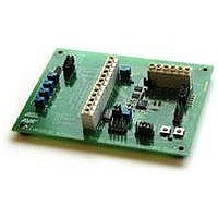
Figure 2-2. SB100 with connectors highlighted
HDR2 provides access to the JTAG interface of the ATmega406, which is used for
programming and debugging using the JTAGICE mkII. The use of JTAGICE mkII is
described in the AVR Studio® online Users Guide and on the Atmel web. Note that
the older JTAGICE does not work with this board.
If the emulator is not required, the I/O signals present here can be used for other
purposes.
Table 2-1. HDR2: JTAG Port
Pin
1
2
3
4
5
6
7
8
9
10
Name
PB3 / TCK
GND
PB0 / TDO
VTref
PB2 / TMS
/RESET
Vsupply
n/c
PB1 / TDI
GND
Direction
I/O
I/O
Output
I/O
Input
Output
I/O
Usage
TCK JTAG signal
TDO JTAG signal
+3.3V reference
TMS JTAG signal
Reset signal
+3.3V
TDI JTAG signal
A – JB3
B – CONN2
C – CONN1
D – J1
E – JB1
F – HDR2
G – JB4
H – HDR1
I – JB2
AVR454
3
Related parts for ATAVRSB100
Image
Part Number
Description
Manufacturer
Datasheet
Request
R

Part Number:
Description:
DEV KIT FOR AVR/AVR32
Manufacturer:
Atmel
Datasheet:

Part Number:
Description:
INTERVAL AND WIPE/WASH WIPER CONTROL IC WITH DELAY
Manufacturer:
ATMEL Corporation
Datasheet:
Part Number:
Description:
Low-Voltage Voice-Switched IC for Hands-Free Operation
Manufacturer:
ATMEL Corporation
Datasheet:
Part Number:
Description:
MONOLITHIC INTEGRATED FEATUREPHONE CIRCUIT
Manufacturer:
ATMEL Corporation
Datasheet:
Part Number:
Description:
AM-FM Receiver IC U4255BM-M
Manufacturer:
ATMEL Corporation
Datasheet:
Part Number:
Description:
Monolithic Integrated Feature Phone Circuit
Manufacturer:
ATMEL Corporation
Datasheet:
Part Number:
Description:
Multistandard Video-IF and Quasi Parallel Sound Processing
Manufacturer:
ATMEL Corporation
Datasheet:
Part Number:
Description:
High-performance EE PLD
Manufacturer:
ATMEL Corporation
Datasheet:
Part Number:
Description:
8-bit Flash Microcontroller
Manufacturer:
ATMEL Corporation
Datasheet:
Part Number:
Description:
2-Wire Serial EEPROM
Manufacturer:
ATMEL Corporation
Datasheet: