ATAVRSB100 Atmel, ATAVRSB100 Datasheet - Page 9
ATAVRSB100
Manufacturer Part Number
ATAVRSB100
Description
SMART BATTERY DEVELOPMENT KIT
Manufacturer
Atmel
Type
Smart Batteryr
Datasheet
1.ATAVRSB100.pdf
(20 pages)
Specifications of ATAVRSB100
Contents
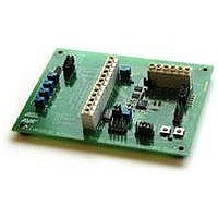
Fully Assembled Evaluation Board
Processor
ATmega406
Processor To Be Evaluated
ATmega406
Data Bus Width
8 bit
Interface Type
JTAG
For Use With/related Products
ATmega406
Lead Free Status / RoHS Status
Contains lead / RoHS non-compliant
Other names
Q2367281


2.2.2 Simulating Charging and Discharging
2.2.3 Simulating Cell Imbalance
2.2.4 Current Simulation
2598C-AVR-06/06
When working on packs that use either a 2-cell or a 3-cell stack, the potentiometers
for cells 3 and 4 (or just cell4) should be adjusted to their minimum setting. This will
reduce the required voltage at the power supply accordingly, and will also accurately
reflect the behavior that will be seen in the final design. Note that the #define
parameters in cell.h should be adjusted accordingly to prevent the software from
detecting this as an under-voltage condition on cell 3 or cell 4.
VR5, after calibration, will adjust all cell simulation voltages together. If V-SIM1-4
have been adjusted to match, they will track each other very accurately while VR5 is
adjusted.
In most cases, then, adjusting VR5 by itself will be all that is required when simulating
charging and discharging. If V-SIM1-4 have been adjusted to match, then it will only
be necessary to monitor the total stack voltage and not individual cell voltages.
When monitoring the stack voltage, readings should be taken from the CELL1-
terminal to the highest cell’s positive terminal. Readings should not be taken from the
power supply, as this does not reflect the simulated cell voltages.
Note that VR5 allows the voltage of the stack to be adjusted very low, simulating
severely over-discharged cells. While doing this on the board, the ATmega406 is still
able to operate, but in a final design the ATmega406 operating voltage would be
reduced to the point where the device itself would stop functioning.
Each cell’s adjustment can be brought slightly higher or lower to simulate cell
imbalance without affecting the other cells. Note that the adjustment is fairly sensitive,
so a light touch on the cell’s potentiometer is better. The voltage of any given cell may
be monitored at the CELLx terminals on CONN2.
To use the current simulation circuitry, set the jumpers on JB4 for I-SIM mode as
shown in Figure 2-3, and connect a regulated, accurate 5.0VDC supply to the
designated I-SIM terminals on CONN2. The polarity of the supply will determine
whether you are simulating Charging or Discharging. Specifically, if the I-SIM+/-5V
terminal is positive, you will be simulating Charging.
Adjusting VR6 (I-SIM ADJ) will now vary the voltage present at the ATmega406
PPI/PI/NI/NNI terminals. Rotating VR6 clockwise will increase the magnitude of the
voltage present, but the polarity will be determined by the wiring of the power supply.
Note that the CCADC can tolerate up to +/-0.22V, but is only specified to read in the
range of +/-0.15V. Although adjusting VR6 fully may result in a voltage greater than
0.15V, this will not damage the ATmega406 device.
The simulated voltage can be measured at JB4, pins 3 and 4. Note that the amount of
current indicated by this voltage will be dependent on the value of the sense resistor
you use in your final design.
Since most connected systems are constant-power, when simulating discharge by
means of reducing the cell voltage you should also increase the setting of VR6 to
simulate higher current.
AVR454
9
Related parts for ATAVRSB100
Image
Part Number
Description
Manufacturer
Datasheet
Request
R

Part Number:
Description:
DEV KIT FOR AVR/AVR32
Manufacturer:
Atmel
Datasheet:

Part Number:
Description:
INTERVAL AND WIPE/WASH WIPER CONTROL IC WITH DELAY
Manufacturer:
ATMEL Corporation
Datasheet:
Part Number:
Description:
Low-Voltage Voice-Switched IC for Hands-Free Operation
Manufacturer:
ATMEL Corporation
Datasheet:
Part Number:
Description:
MONOLITHIC INTEGRATED FEATUREPHONE CIRCUIT
Manufacturer:
ATMEL Corporation
Datasheet:
Part Number:
Description:
AM-FM Receiver IC U4255BM-M
Manufacturer:
ATMEL Corporation
Datasheet:
Part Number:
Description:
Monolithic Integrated Feature Phone Circuit
Manufacturer:
ATMEL Corporation
Datasheet:
Part Number:
Description:
Multistandard Video-IF and Quasi Parallel Sound Processing
Manufacturer:
ATMEL Corporation
Datasheet:
Part Number:
Description:
High-performance EE PLD
Manufacturer:
ATMEL Corporation
Datasheet:
Part Number:
Description:
8-bit Flash Microcontroller
Manufacturer:
ATMEL Corporation
Datasheet:
Part Number:
Description:
2-Wire Serial EEPROM
Manufacturer:
ATMEL Corporation
Datasheet: