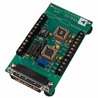
AD2S90-EB Analog Devices Inc, AD2S90-EB Datasheet

AD2S90-EB
Specifications of AD2S90-EB
Related parts for AD2S90-EB
AD2S90-EB Summary of contents
Page 1
... Encoder Emulation Automotive Motion Sensing and Control Factory Automation Limit Switching GENERAL DESCRIPTION The AD2S90 is a complete 12-bit resolution tracking resolver- to-digital converter. No external components are required to operate the device. The converter accepts 2 V rms 10% input signals in the range 3 kHz–20 kHz on the SIN, COS and REF inputs. A Type II ...
Page 2
... AD2S90–SPECIFICATIONS Parameter SIGNAL INPUTS Voltage Amplitude Frequency Input Bias Current Input Impedance 1 Common-Mode Volts CMRR REFERENCE INPUT Voltage Amplitude Frequency Input Bias Current Input Impedance Permissible Phase Shift CONVERTER DYNAMICS Bandwidth Maximum Tracking Rate Maximum VCO Rate (CLKOUT) Settling Time ...
Page 3
... Max Units Test Conditions/Notes 200 ns DIR to CLKOUT Positive Edge 400 ns CLKOUT Pulsewidth 250 ns CLKOUT Negative Edge and NM Transition –3– AD2S90 = – +85 C unless LSB t 7 Test Conditions/Notes CS to DATA Enable CS to 1st SCLK Negative Edge SCLK Low Pulse SCLK High Pulse ...
Page 4
... CAUTION The AD2S90 features an input protection circuit consisting of large “distributed” diodes and polysilicon series resistors to dissipate both high energy discharges (Human Body Model) and fast, low energy pulses (Charges Device Model). Proper ESD precautions are strongly recommended to avoid functional damage or performance degradation ...
Page 5
... E = rotor excitation amplitude O Principle of Operation The AD2S90 operates on a Type 2 tracking closed-loop prin- ciple. The output continually tracks the position of the resolver without the need for external convert and wait states. As the transducer moves through a position equivalent to the least significant bit weighting, the output is updated by one LSB. ...
Page 6
... A 1024 line laser-based encoder will have a maximum speed of 7300 rpm. The inclusion outputs allows the AD2S90 + resolver solution to replace optical encoders directly without the need to change or upgrade existing application software. ...
Page 7
... In this mode the ADSP-2105 provides a CS and a AD2S90 SOLVER serial clock to the AD2S90. The serial clock is inverted to pre- vent timing errors as a result of both the AD2S90 and ADSP- 2105 clock data on the negative edge of SCLK. The first data bit is void; 12 bits of significant data then follow on each con- secutive negative edge of the clock ...
Page 8
... In most data acquisition or control systems the A, B incremental outputs must be decoded into absolute information, normally a parallel word, before they can be utilized effectively. To decode the A, B outputs on the AD2S90 the user must implement a 4 decoding architecture. The principle states that one A, B cycle represents 4 LSB weighted increments of the converter (see Equation 4 • ...
Page 9
... VCO/counter perform the two integrations inher- ent in a Type 2 loop. The overall system response of the AD2S90 is that of a unity gain second order low-pass filter, with the angle of the resolver as the input and the digital position data as the output. Figure 17 illustrates the AD2S90 system diagram ...
Page 10
... Angular Error K K can be used to predict the output position error for a given a input acceleration. The AD2S90 has a fixed K –2 sec if we apply an input accelerating at 100 revs/sec can be calculated as follows: Error in LSBs ...
Page 11
... AD2S90 AGND pin. The SYNREF output of the AD2S99 should be connected to the REF input pin of the AD2S90 via a 0.1 F capacitor with a 100 k resistor to GND. This is to block out any dc offset in the SYNREF signal. For more detailed information please refer to the AD2S99 data sheet ...
Page 12
... AD2S90 0.048 (1.21) 0.042 (1.07) OUTLINE DIMENSIONS Dimensions shown in inches and (mm). P-20A 20-Lead Plastic Leaded Chip Carrier (PLCC) 0.180 (4.57) 0.165 (4.19) 0.048 (1.21) 0.056 (1.42) 0.042 (1.07) 0.025 (0.63) 0.042 (1.07) 0.015 (0.38 0.021 (0.53 PIN 1 0.050 0.013 (0.33) 0.330 (8.38) IDENTIFIER (1 ...


