AD6645-105/PCB Analog Devices Inc, AD6645-105/PCB Datasheet - Page 6
AD6645-105/PCB
Manufacturer Part Number
AD6645-105/PCB
Description
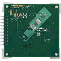
BOARD EVAL ADC 105MSPS AD6645
Manufacturer
Analog Devices Inc
Series
SoftCell®r
Datasheet
1.AD6645ASVZ-80.pdf
(24 pages)
Specifications of AD6645-105/PCB
Rohs Status
RoHS non-compliant
Design Resources
Low Jitter Sampling Clock Generator for High Performance ADCs Using AD9958/9858 and AD9515 (CN0109)
Number Of Adc's
1
Number Of Bits
14
Sampling Rate (per Second)
105M
Data Interface
Parallel
Inputs Per Adc
1 Differential
Input Range
2.2 Vpp
Power (typ) @ Conditions
1.5W @ 105MSPS
Voltage Supply Source
Analog and Digital
Operating Temperature
-10°C ~ 85°C
Utilized Ic / Part
AD6645 105MSPS


AD6645
Parameter
DATA-READY (DRY
APERTURE DELAY
APERTURE UNCERTAINTY (JITTER)
1
2
3
4
5
Several timing parameters are a function of t
Several timing parameters are a function of t
ENCODE TO DATA Delay (Hold Time) is the absolute minimum propagation delay through the ADC, t
DRY is an inverted and delayed version of the encode clock. Any change in the duty cycle of the clock will correspondingly change the duty cycle of DRY.
Data-ready to DATA Delay (t
Data-Ready to DATA Delay (Hold Time)
Data-Ready to DATA Delay (Setup Time)
50% Duty Cycle
50% Duty Cycle
4
)/DATA(D13:0),, OVR
H_DR
and t
D[13:0], OVR
S_DR
ENCODE,
ENCODE
) is calculated relative to rated speed grade and is dependent on t
DRY
AIN
t
ENC
ENCL
E_RL
and t
and t
t
A
Symbol
t
t
t
t
H_DR
S_DR
A
J
N
ENCH
N
ENCH
t
.
.
ENC
t
E_FL
N – 3
Temp
Full
Full
Full
Full
25°C
25°C
t
N + 1
ENCH
N + 1
Figure 2. Timing Diagram
Rev. D | Page 6 of 24
Test
Level
V
V
V
V
V
V
t
ENCL
N – 2
t
DR
N + 2
Min
6.6
2.1
N + 2
t
E_DR
t
S_DR
AD6645ASQ-80/
AD6645ASV-80
N – 1
Typ
Note 5
7.2
Note 5
3.6
−500
0.1
t
H_DR
E_RL
N + 3
N + 3
t
S_E
= t
5
5
ENC
H_E
and duty cycle.
.
Max
7.9
5.1
N
N + 4
N + 4
Min
5.1
0.6
0.1
t
H_E
AD6645ASQ-105/
AD6645ASV-105
Typ
Note 5
5.7
Note 5
2.1
−500
5
5
Max
6.4
3.5
Unit
ns
ns
ps
ps rms
Related parts for AD6645-105/PCB
Image
Part Number
Description
Manufacturer
Datasheet
Request
R

Part Number:
Description:
BOARD EVAL ADC 80MSPS AD6645
Manufacturer:
Analog Devices Inc
Datasheet:
Part Number:
Description:
BOARD EVAL AD6645-MIL/PCB
Manufacturer:
Analog Devices Inc
Datasheet:

Part Number:
Description:
BOARD EVAL ADC 80MSPS AD6645
Manufacturer:
Analog Devices Inc
Datasheet:

Part Number:
Description:
14-Bit, 80 MSPS/105 MSPS A/D Converter
Manufacturer:
Analog Devices
Datasheet:
Part Number:
Description:
14-Bit, 80 MSPS Analog to Digital Converter
Manufacturer:
Analog Devices
Part Number:
Description:
14-Bit/ 80 MSPS A/D Converter
Manufacturer:
Analog Devices
Datasheet:

Part Number:
Description:
±1.7g Dual-Axis IMEMS Accelerometer Evaluation Board
Manufacturer:
Analog Devices Inc
Datasheet:
Part Number:
Description:
Inertial Sensor Evaluation System
Manufacturer:
Analog Devices Inc
Datasheet:
Part Number:
Description:
Manufacturer:
Analog Devices Inc
Datasheet:
Part Number:
Description:
Manufacturer:
Analog Devices Inc
Datasheet:
Part Number:
Description:
Manufacturer:
Analog Devices Inc
Datasheet:
Part Number:
Description:
Manufacturer:
Analog Devices Inc
Datasheet:
Part Number:
Description:
Manufacturer:
Analog Devices Inc
Datasheet: