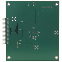
AD9433/PCB Analog Devices Inc, AD9433/PCB Datasheet

AD9433/PCB
Specifications of AD9433/PCB
Related parts for AD9433/PCB
AD9433/PCB Summary of contents
Page 1
FEATURES IF sampling up to 350 MHz SNR: 67.5 dB Nyquist at 105 MSPS IN SFDR: 83 dBc MHz at 105 MSPS IN SFDR: 72 dBc 150 MHz at 105 MSPS IN ...
Page 2
AD9433 TABLE OF CONTENTS Features .............................................................................................. 1 Applications ....................................................................................... 1 General Introduction ....................................................................... 1 Functional Block Diagram .............................................................. 1 Product Highlights ........................................................................... 1 Revision History ............................................................................... 2 Specifications ..................................................................................... 3 DC Specifications ......................................................................... 3 AC Specifications .......................................................................... 4 Switching Specifications ...
Page 3
SPECIFICATIONS DC SPECIFICATIONS internal reference; differential encode input, unless otherwise noted Table 1. Parameter Temp RESOLUTION ACCURACY No Missing Codes Full Offset Error Full 1 Gain Error 25°C 2 Differential ...
Page 4
AD9433 Parameter Temp DIGITAL OUTPUTS Logic 1 Voltage Full Logic 0 Voltage Full Output Coding 1 Gain error and gain temperature coefficients are based on the ADC only (with a fixed 2.5 V external reference and p-p ...
Page 5
SWITCHING SPECIFICATIONS differential encode input, unless otherwise noted Table 3. Parameter Encode Rate Encode Pulse Width High ( Encode Pulse Width Low ( Aperture Delay (t ...
Page 6
AD9433 ABSOLUTE MAXIMUM RATINGS Table 4. Parameter Analog Inputs Digital Inputs Digital Output Current Operating Temperature Range ( Storage Temperature Range Maximum Junction Temperature ( Stresses above those listed under Absolute Maximum ...
Page 7
PIN CONFIGURATION AND FUNCTION DESCRIPTIONS Table 6. Pin Function Descriptions Pin No. Mnemonic 11, 33, GND 34, 35, 38, 39, 40, 43, 48 10, 36, 37 44, 47 ...
Page 8
AD9433 TYPICAL PERFORMANCE CHARACTERISTICS 0 SNR = 67.5dB –10 SFDR = 85dBFS –20 –30 –40 –50 –60 –70 –80 –90 –100 –110 –120 0 13.1 26.3 FREQUENCY (MHz) Figure 4. FFT 105 MSPS 49.3 MHz, Differential ...
Page 9
IMD3 = 92dBFS –10 –20 –30 –40 –50 –60 –70 –80 –90 –100 –110 –120 0 7.5 15.0 22.5 30.0 FREQUENCY (MHz) Figure 10. FFT 105 MSPS 49.3 MHz and 50.3 MHz Differential ...
Page 10
AD9433 –95 WORST OTHER (dBc) –90 THIRD HARMONIC (dBc) –85 –80 SECOND HARMONIC (dBc) –75 SNR (dB) –70 – DUTY CYCLE HIGH (%) Figure 16. Dynamic Performance vs. Encode Duty Cycle ...
Page 11
SNR = 66.8dB –10 SFDR = 83dBFS –20 –30 –40 –50 –60 –70 –80 –90 –100 –110 –120 0 7.5 15.0 22.5 30.0 FREQUENCY (MHz) Figure 22. FFT 105 MSPS 70.3 MHz, Differential AIN @ ...
Page 12
AD9433 0 SNR = 64dB –10 SFDR = 78dBFS –20 –30 –40 –50 –60 –70 –80 –90 –100 –110 –120 0 7.5 15.0 22.5 30.0 FREQUENCY (MHz) Figure 28. FFT 105 MSPS 150.3 MHz, Differential AIN ...
Page 13
FREQUENCY (MHz) Figure 34. FFT 76.8 MSPS 59.6 MHz, Two WCDMA Carriers Differential AIN, SFDR Mode Enabled 0 ...
Page 14
AD9433 TERMINOLOGY Analog Bandwidth The analog input frequency at which the spectral power of the fundamental frequency (as determined by the FFT analysis) is reduced by 3 dB. Aperture Delay The delay between the 50% point of the rising edge ...
Page 15
Spurious-Free Dynamic Range (SFDR) The ratio of the rms signal amplitude to the rms value of the peak spurious spectral component. The peak spurious compo- nent may or may not be a harmonic. May be reported in dBc (degrades as ...
Page 16
AD9433 EQUIVALENT CIRCUITS V CC VREFIN Figure 36. Voltage Reference Input Circuit V CC 3.75kΩ 3.75kΩ AIN AIN 15kΩ 15kΩ Figure 37. Analog Input Circuit Figure 38. Digital Output Circuit V Figure 39. Voltage Reference Output Circuit ...
Page 17
THEORY OF OPERATION The AD9433 is a 12-bit pipeline converter that uses a switched- capacitor architecture. Optimized for high speed, this converter provides flat dynamic performance up to and beyond the Nyquist limit. DNL transitional errors are calibrated at final ...
Page 18
AD9433 ANALOG INPUT The analog input to the AD9433 is a differential buffer. The input buffer is self-biased by an on-chip resistor divider that sets the dc common-mode voltage to a nominal 4 V (see the Equivalent Circuits section). Rated ...
Page 19
APPLICATIONS INFORMATION LAYOUT INFORMATION A multilayer board is recommended to achieve best results highly recommended that high quality, ceramic chip capacitors be used to decouple each supply pin to ground directly at the device. The pinout of the ...
Page 20
AD9433 OUTLINE DIMENSIONS 1.20 0.75 MAX 0.60 0.45 SEATING PLANE 0° MIN 1.05 0.20 1.00 0.09 0.95 7° 3.5° 0.15 0° 0.05 0.08 MAX COPLANARITY VIEW A ROTATED 90 ° CCW ORDERING GUIDE Model Temperature Range 1 AD9433BSVZ-105 −40°C to ...


