EVAL-AD7490CB Analog Devices Inc, EVAL-AD7490CB Datasheet
EVAL-AD7490CB
Specifications of EVAL-AD7490CB


Related parts for EVAL-AD7490CB


EVAL-AD7490CB Summary of contents
Page 1
FEATURES Fast throughput rate: 1 MSPS Specified for Low power at maximum throughput rates 5.4 mW maximum at 870 kSPS with 3 V supplies 12.5 mW maximum at 1 MSPS with 5 ...
Page 2
AD7490 TABLE OF CONTENTS Features .............................................................................................. 1 Functional Block Diagram .............................................................. 1 General Description ......................................................................... 1 Product Highlights ........................................................................... 1 Revision History ............................................................................... 2 Specifications ..................................................................................... 3 Timing Specifications .................................................................. 5 Absolute Maximum Ratings ............................................................ 6 ESD Caution .................................................................................. 6 ...
Page 3
SPECIFICATIONS 2 5.25 V, REF = 2 DRIVE IN −40°C to +85°C. Table 1. Parameter DYNAMIC PERFORMANCE 2 Signal-to-(Noise + Distortion) (SINAD) 2 Signal-to-Noise Ratio (SNR) Total Harmonic Distortion (THD) 2 ...
Page 4
AD7490 Parameter LOGIC INPUTS Input High Voltage, V INH Input Low Voltage, V INL Input Current Input Capacitance LOGIC OUTPUTS Output High Voltage Output Low Voltage Floating State Leakage Current ...
Page 5
TIMING SPECIFICATIONS ≤ REF DD DRIVE DD 1 Table 2. Timing Specifications Limit MIN MAX Parameter ...
Page 6
AD7490 ABSOLUTE MAXIMUM RATINGS T = 25°C, unless otherwise noted. A Table 3. Parameter V to GND GND DRIVE Analog Input Voltage to GND Digital Input Voltage to GND Digital Output Voltage to GND REF to GND ...
Page 7
PIN CONFIGURATIONS AND FUNCTION DESCRIPTIONS AD7490 TOP VIEW ...
Page 8
AD7490 TYPICAL PERFORMANCE CHARACTERISTICS Figure 5 shows a typical FFT plot for the AD7490 at 1 MSPS sample rate and 50 kHz input frequency. Figure 7 shows the power supply rejection ratio vs. supply ripple frequency for the AD7490. The ...
Page 9
25°C A – 5.25V DD RANGE = 0V TO REF IN –60 –65 – 100Ω IN – 5Ω IN – 10Ω IN –85 10 100 ...
Page 10
AD7490 TERMINOLOGY Integral Nonlinearity This is the maximum deviation from a straight line passing through the endpoints of the ADC transfer function. The end- points of the transfer function are zero scale, a point 1 LSB below the first code ...
Page 11
Peak Harmonic or Spurious Noise Peak harmonic or spurious noise is defined as the ratio of the rms value of the next largest component in the ADC output spectrum ( and excluding dc) to the rms value ...
Page 12
AD7490 INTERNAL REGISTER STRUCTURE CONTROL REGISTER The control register on the AD7490 is a 12-bit, write-only register. Data is loaded from the DIN pin of the AD7490 on the falling edge of SCLK. The data is transferred on the DIN ...
Page 13
Table 7. Channel Selection ADD3 ADD2 Table 8. ...
Page 14
AD7490 SHADOW REGISTER The Shadow register on the AD7490 is a 16-bit, write-only register. Data is loaded from the DIN pin of the AD7490 on the falling edge of SCLK. The data is transferred on the DIN line at the ...
Page 15
Figure 14 shows how a sequence of consecutive channels can be converted on without having to program the Shadow register or write to the part on each serial transfer. Again, to exit this mode of operation and revert back to ...
Page 16
AD7490 THEORY OF OPERATION CIRCUIT INFORMATION The AD7490 is a fast, 16-channel, 12-bit, single-supply, analog- to-digital converter. The parts can be operated from a 2 5.25 V supply. When operated from supply and provided with ...
Page 17
When no amplifier is used to drive the analog input, the source impedance should be limited to low values. The maximum source impedance depends on the amount of total harmonic distortion (THD) that can be tolerated. The THD increases as ...
Page 18
AD7490 TYPICAL CONNECTION DIAGRAM Figure 21 shows a typical connection diagram for the AD7490. In this setup, the AGND pin is connected to the analog ground plane of the system. In Figure 21, REF IN decoupled 2.5 V supply from ...
Page 19
Reference Section An external reference source should be used to supply the 2.5 V reference to the AD7490. Errors in the reference source result in gain errors in the AD7490 transfer function and add to the specified full-scale errors of ...
Page 20
AD7490 Auto Shutdown (PM1 = 0, PM0 = 1) In this mode, the AD7490 automatically enters shutdown at the end of each conversion when the control register is updated. When the part is in shutdown, the track-and-hold is in hold ...
Page 21
Powering Up the AD7490 When supplies are first applied to the AD7490, the ADC may power up in any of the operating modes of the part. To ensure that the part is placed into the required operating mode, the user ...
Page 22
AD7490 SERIAL INTERFACE Figure 27 shows the detailed timing diagram for serial interfacing to the AD7490. The serial clock provides the conversion clock and also controls the transfer of information to and from the AD7490 during each conversion. The CS ...
Page 23
If the WEAK/ TRI bit in the control register is set to 1, instead of th returning to true three-state on the 16 DOUT line is pulled weakly to the logic level corresponding to ADD3 of the next serial transfer. ...
Page 24
AD7490 MICROPROCESSOR INTERFACING The serial interface on the AD7490 allows the part to be directly connected to a range of many different microprocessors. This section explains how to interface the AD7490 with some of the more common microcontroller and DSP ...
Page 25
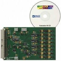
... EVAL-CONTROL BRD2. The EVAL-CONTROL BRD2 can be used in conjunction with the AD7490 evaluation board, as well as many other Analog Devices, Inc., evaluation boards ending in the CB designator, to demonstrate and evaluate the ac and dc performance of the AD7490. The software allows the user to perform ac (fast Fourier transform) and dc (histogram of codes) tests on the AD7490 ...
Page 26
AD7490 OUTLINE DIMENSIONS PIN 1 0.15 0.05 COPLANARITY PIN 1 INDICATOR 12° MAX 1.00 0.85 0.80 SEATING PLANE 9.80 9.70 9. 4.50 4.40 4. 0.65 BSC 1.20 MAX 0.30 0.20 0.19 SEATING 0.09 ...
Page 27
... This board is a complete unit allowing control and communicate with all Analog Devices evaluation boards ending designator. To order a complete evaluation kit, you need to order the particular ADC evaluation board (for example, EVAL-AD7490CBZ), the EVAL-CONTROL-BRD2, and transformer. See the relevant evaluation board data sheet for more information. ...
Page 28
AD7490 NOTES ©2002–2009 Analog Devices, Inc. All rights reserved. Trademarks and registered trademarks are the property of their respective owners. D02691-0-6/09(C) Rev Page ...