EVAL-AD7490CB Analog Devices Inc, EVAL-AD7490CB Datasheet - Page 12
EVAL-AD7490CB
Manufacturer Part Number
EVAL-AD7490CB
Description
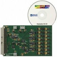
BOARD EVAL FOR AD7490
Manufacturer
Analog Devices Inc
Datasheet
1.AD7490BRUZ.pdf
(28 pages)
Specifications of EVAL-AD7490CB
Number Of Adc's
1
Number Of Bits
12
Sampling Rate (per Second)
1M
Data Interface
Serial
Inputs Per Adc
16 Single Ended
Input Range
0 ~ 5 V
Power (typ) @ Conditions
12.5mW @ 1MSPS, 5 V
Voltage Supply Source
Single
Operating Temperature
-40°C ~ 85°C
Utilized Ic / Part
AD7490
Lead Free Status / RoHS Status
Contains lead / RoHS non-compliant


AD7490
INTERNAL REGISTER STRUCTURE
CONTROL REGISTER
The control register on the AD7490 is a 12-bit, write-only
register. Data is loaded from the DIN pin of the AD7490 on the
falling edge of SCLK. The data is transferred on the DIN line at
the same time as the conversion result is read from the part.
The data transferred on the DIN line corresponds to the
Table 5. Control Register
MSB
11
WRITE
Table 6. Control Register Bit Functions
Bit
11
10
9 to 6
5, 4
3
2
1
0
Name
WRITE
SEQ
ADD3 to
ADD0
PM1, PM0
SHADOW
WEAK/TRI
RANGE
CODING
10
SEQ
9
ADD3
Description
The value written to this bit of the control register determines whether the following 11 bits are loaded to the
control register or not. If this bit is a 1, the following 11 bits are written to the control register; if it is a 0, the
remaining 11 bits are not loaded to the control register, and it remains unchanged.
The SEQ bit in the control register is used in conjunction with the SHADOW bit to control the use of the sequencer
function and access the Shadow register (see Table 9).
These four address bits are loaded at the end of the present conversion sequence and select which analog input
channel is to be converted on in the next serial transfer, or they may select the final channel in a consecutive
sequence, as described in Table 9. The selected input channel is decoded as shown in Table 7. The next channel to
be converted on is selected by the mux on the 14
conversion result are also output on DOUT prior to the 12 bits of data (see the Serial Interface section).
Power management bits. These two bits decode the mode of operation of the AD7490, as shown in Table 8.
The SHADOW bit in the control register is used in conjunction with the SEQ bit to control the use of the sequencer
function and access the Shadow register (see Table 9).
This bit selects the state of the DOUT line at the end of the current serial transfer. If it is set to 1, the DOUT line is
weakly driven to the ADD3 channel address bit of the ensuing conversion. If this bit is set to 0, DOUT returns to
three-state at the end of the serial transfer. See the Control Register section for more details.
This bit selects the analog input range to be used on the AD7490. If it is set to 0, the analog input range extends
from 0 V to 2 × REF
For 0 V to 2 × REF
This bit selects the type of output coding used by the AD7490 for the conversion result. If this bit is set to 0, the
output coding for the part is twos complement. If this bit is set to 1, the output coding from the part is straight
binary (for the next conversion).
8
ADD2
7
ADD1
IN
, V
IN
. If it is set to 1, the analog input range extends from 0 V to REF
DD
= 4.75 V to 5.25 V.
6
ADD0
Rev. C | Page 12 of 28
5
PM1
4
PM0
AD7490 configuration for the next conversion. This requires
16 serial clocks for every data transfer. Only the information
provided on the first 12 falling clock edges (after the CS falling
edge) is loaded to the control register. MSB denotes the first bit
in the data stream. The bit functions are outlined in
th
SCLK falling edge. The address bits corresponding to the
3
SHADOW
2
WEAK/TRI
IN
(for the next conversion).
1
RANGE
Table 5
LSB
0
CODING
.
Related parts for EVAL-AD7490CB
Image
Part Number
Description
Manufacturer
Datasheet
Request
R

Part Number:
Description:
ENERCHIP CC EVAL KIT
Manufacturer:
Cymbet Corporation
Datasheet:

Part Number:
Description:
BOARD EVAL FOR AD976
Manufacturer:
Analog Devices Inc
Datasheet:

Part Number:
Description:
BOARD EVAL FOR ADXL345
Manufacturer:
Analog Devices Inc
Datasheet:

Part Number:
Description:
ENERCHIP CC SEH EVAL KIT
Manufacturer:
Cymbet Corporation
Datasheet:

Part Number:
Description:
ENERCHIP EP ENERGY HARVEST EVAL
Manufacturer:
Cymbet Corporation
Datasheet:

Part Number:
Description:
EVAL BOARD FOR TW6864-LB2-GR
Manufacturer:
Intersil
Datasheet:
Part Number:
Description:
EVAL BOARD FOR TW8816-LB3-GR
Manufacturer:
Intersil
Datasheet:
Part Number:
Description:
EVAL BOARD FOR TW8817-TA3-GRS
Manufacturer:
Intersil
Datasheet:

Part Number:
Description:
EVALUATION MODULE FOR ADUM4160
Manufacturer:
Analog Devices Inc
Datasheet:

Part Number:
Description:
BOARD EVALUATION ADCMP581BCP
Manufacturer:
Analog Devices Inc
Datasheet:
Part Number:
Description:
BOARD EVALUATION ADM1041
Manufacturer:
Analog Devices Inc
Datasheet:

Part Number:
Description:
EVAL BOARD FOR STM32F107VCT
Manufacturer:
STMicroelectronics
Datasheet:
Part Number:
Description:
BOARD EVAL FOR AD1954
Manufacturer:
Analog Devices Inc
Datasheet:
Part Number:
Description:
BOARD EVAL FOR AD1955
Manufacturer:
Analog Devices Inc
Datasheet:

Part Number:
Description:
BOARD EVAL FOR AD7655
Manufacturer:
Analog Devices Inc
Datasheet: