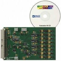
EVAL-AD7490CB Analog Devices Inc, EVAL-AD7490CB Datasheet - Page 13

EVAL-AD7490CB
Manufacturer Part Number
EVAL-AD7490CB
Description
BOARD EVAL FOR AD7490
Manufacturer
Analog Devices Inc
Datasheet
1.AD7490BRUZ.pdf
(28 pages)
Specifications of EVAL-AD7490CB
Number Of Adc's
1
Number Of Bits
12
Sampling Rate (per Second)
1M
Data Interface
Serial
Inputs Per Adc
16 Single Ended
Input Range
0 ~ 5 V
Power (typ) @ Conditions
12.5mW @ 1MSPS, 5 V
Voltage Supply Source
Single
Operating Temperature
-40°C ~ 85°C
Utilized Ic / Part
AD7490
Lead Free Status / RoHS Status
Contains lead / RoHS non-compliant
Table 7. Channel Selection
ADD3
0
0
0
0
0
0
0
0
1
1
1
1
1
1
1
1
Table 8. Power Mode Selection
PM1
1
1
0
0
Sequencer Operation
The configuration of the SEQ and SHADOW bits in the control register allows the user to select a particular mode of operation of the
sequencer function. Table 9 outlines the four modes of operation of the sequencer.
Table 9. Sequence Selection
SEQ
0
0
1
1
SHADOW
0
1
0
1
PM0
1
0
1
0
Mode
Normal operation. In this mode, the AD7490 remains in full power mode, regardless of the status of any of the logic inputs.
This mode allows the fastest possible throughput rate from the AD7490.
Full shutdown. In this mode, the AD7490 is in full shutdown mode, with all circuitry on the AD7490 powering down. The
AD7490 retains the information in the control register while in full shutdown. The part remains in full shutdown until these
bits are changed in the control register.
Auto shutdown. In this mode, the AD7490 automatically enters shutdown mode at the end of each conversion when the
control register is updated. Wake-up time from shutdown is 1 μs, and the user should ensure that 1 μs has elapsed before
attempting to perform a valid conversion on the part in this mode.
Auto standby. In this standby mode, portions of the AD7490 are powered down, but the on-chip bias generator remains
powered up. This mode is similar to auto shutdown and allows the part to power up within one dummy cycle, that is, 1 μs
with a 20 MHz SCLK.
Sequence Type
This configuration means the sequence function is not used. The analog input channel selected for each individual
conversion is determined by the contents of the channel address bits ADD0 through ADD3 in each prior write
operation. This mode of operation reflects the normal operation of a multichannel ADC, without the sequencer
function being used, where each write to the AD7490 selects the next channel for conversion (see Figure 12).
This configuration selects the Shadow register for programming. After the write to the control register, the following
write operation loads the contents of the Shadow register. This programs the sequence of channels to be converted on
continuously with each successive valid CS falling edge (see Shadow register,
selected need not be consecutive.
If the SEQ and SHADOW bits are set in this way, the sequence function is not interrupted upon completion of the write
operation. This allows other bits in the control register to be altered while in a sequence without terminating the cycle.
This configuration is used in conjunction with the ADD3 to ADD0 channel address bits to program continuous
conversions on a consecutive sequence of channels from Channel 0 through to a selected final channel, as determined
by the channel address bits in the control register (see Figure 14).
ADD2
0
0
0
0
1
1
1
1
0
0
0
0
1
1
1
1
ADD1
0
0
1
1
0
0
1
1
0
0
1
1
0
0
1
1
Rev. C | Page 13 of 28
ADD0
0
1
0
1
0
1
0
1
0
1
0
1
0
1
0
1
Analog Input Channel
V
V
V
V
V
V
V
V
V
V
V
V
V
V
V
V
IN
IN
IN
IN
IN
IN
IN
IN
IN
IN
IN
IN
IN
IN
IN
IN
0
1
2
3
4
5
6
7
8
9
10
11
12
13
14
15
Table 10
and
Figure 13
). The channels
AD7490


