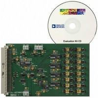
EVAL-AD7490CB Analog Devices Inc, EVAL-AD7490CB Datasheet - Page 14

EVAL-AD7490CB
Manufacturer Part Number
EVAL-AD7490CB
Description
BOARD EVAL FOR AD7490
Manufacturer
Analog Devices Inc
Datasheet
1.AD7490BRUZ.pdf
(28 pages)
Specifications of EVAL-AD7490CB
Number Of Adc's
1
Number Of Bits
12
Sampling Rate (per Second)
1M
Data Interface
Serial
Inputs Per Adc
16 Single Ended
Input Range
0 ~ 5 V
Power (typ) @ Conditions
12.5mW @ 1MSPS, 5 V
Voltage Supply Source
Single
Operating Temperature
-40°C ~ 85°C
Utilized Ic / Part
AD7490
Lead Free Status / RoHS Status
Contains lead / RoHS non-compliant
AD7490
SHADOW REGISTER
The Shadow register on the AD7490 is a 16-bit, write-only
register. Data is loaded from the DIN pin of the AD7490 on the
falling edge of SCLK. The data is transferred on the DIN line at
the same time that a conversion result is read from the part.
This requires 16 serial falling edges for the data transfer. The
information is clocked into the Shadow register, provided the
SEQ and SHADOW bits are set to 0, 1, respectively, in the
previous write to the control register. MSB denotes the first bit
in the data stream. Each bit represents an analog input from
Channel 0 through Channel 15. A sequence of channels can be
selected through which the AD7490 cycles with each consecutive
CS falling edge after the write to the Shadow register. To select a
sequence of channels, the associated channel bit must be set for
each analog input. The AD7490 continuously cycles through
the selected channels in ascending order, beginning with the
lowest channel, until a write operation occurs (that is, the WRITE
bit is set to 1), with the SEQ and SHADOW bits configured in
any way except 1, 0 (see
in
Figure 12 reflects the normal operation of a multichannel ADC,
where each serial transfer selects the next channel for conversion.
In this mode of operation, the sequencer function is not used.
CS
CS
Table 10. Shadow Register
MSB
15
V
IN
Table 10
0
14
V
IN
DIN: WRITE TO CONTROL REGISTER,
WRITE BIT = 1,
SELECT CODING, RANGE, AND POWER MODE
SELECT CHANNEL ADD3 TO ADD0 FOR
CONVERSION,
SEQ = SHADOW = 0
DOUT: CONVERSION RESULT FROM
PREVIOUSLY SELECTED CHANNEL ADD3 TO
ADD0
DIN: WRITE TO CONTROL REGISTER,
WRITE BIT = 1,
SELECT CODING, RANGE,AND POWER MODE
SELECT ADD3 TO ADD0 FOR CONVERSION,
SEQ = SHADOW = 0
.
1
Figure 12. SEQ Bit = 0, SHADOW Bit = 0 Flowchart
13
V
IN
DUMMY CONVERSIONS
DIN = ALL 1s
2
POWER ON
Table 9
V
12
IN
3
). The bit functions are outlined
11
V
IN
4
10
V
IN
5
WRITE BIT = 1,
SEQ = SHADOW = 0
9
V
IN
6
8
V
IN
Rev. C | Page 14 of 28
7
7
V
IN
8
CS
Figure 13 shows how to program the AD7490 to continuously
convert on a particular sequence of channels using the Shadow
register. To exit this mode of operation and revert back to the
normal mode of operation of a multichannel ADC (as outlined
in Figure 12), ensure that WRITE = 1 and SEQ = SHADOW = 0
on the next serial transfer.
6
V
IN
WRITE
BIT = 0
CS
CS
9
5
V
IN
Figure 13. SEQ Bit = 0, SHADOW Bit = 1 Flowchart
10
CONTINUOUSLY
CONVERTS ON THE
SELECTED SEQUENCE
OF CHANNELS
DIN: WRITE TO CONTROL REGISTER,
WRITE BIT = 1,
SELECT CODING, RANGE, AND POWER MODE
SELECT CHANNEL ADD3 TO ADD0 FOR
CONVERSION,
SEQ = 0 SHADOW = 1
DOUT: CONVERSION RESULT FROM
PREVIOUSLY SELECTED CHANNEL ADD3 TO
ADD0
DIN: WRITE TO SHADOW REGISTER,
SELECTING WHICH CHANNELS TO CONVERT
ON; CHANNELS SELECTED NEED NOT BE
CONSECUTIVE
WRITE BIT = 0
4
V
WRITE BIT = 0
IN
11
DUMMY CONVERSIONS
DIN = ALL 1s
POWER ON
3
V
IN
12
CONTINUOUSLY
CONVERTS ON THE
SELECTED SEQUENCE
OF CHANNELS BUT
ALLOWS RANGE,
CODING, AND SO ON,
TO CHANGE IN THE
CONTROL REGISTER
WITHOUT
INTERRUPTING THE
SEQUENCE PROVIDED,
SEQ = 1 SHADOW = 0
WRITE BIT = 1,
SEQ = 1, SHADOW = 0
2
V
IN
13
WRITE BIT = 1,
SEQ = 1,
SHADOW = 0
1
V
IN
14
LSB
0
V
IN
15


