EVAL-AD7490CB Analog Devices Inc, EVAL-AD7490CB Datasheet - Page 24
EVAL-AD7490CB
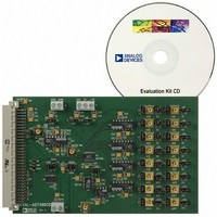
Manufacturer Part Number
EVAL-AD7490CB
Description
BOARD EVAL FOR AD7490
Manufacturer
Analog Devices Inc
Datasheet
1.AD7490BRUZ.pdf
(28 pages)
Specifications of EVAL-AD7490CB
Number Of Adc's
1
Number Of Bits
12
Sampling Rate (per Second)
1M
Data Interface
Serial
Inputs Per Adc
16 Single Ended
Input Range
0 ~ 5 V
Power (typ) @ Conditions
12.5mW @ 1MSPS, 5 V
Voltage Supply Source
Single
Operating Temperature
-40°C ~ 85°C
Utilized Ic / Part
AD7490
Lead Free Status / RoHS Status
Contains lead / RoHS non-compliant


AD7490
MICROPROCESSOR INTERFACING
The serial interface on the AD7490 allows the part to be directly
connected to a range of many different microprocessors. This
section explains how to interface the AD7490 with some of the
more common microcontroller and DSP serial interface
protocols.
AD7490 to TMS320C541
The serial interface on the TMS320C541 uses a continuous serial
clock and frame synchronization signals to synchronize the data
transfer operations with peripheral devices like the AD7490.
The CS input allows easy interfacing between the TMS320C541
and the AD7490 without any glue logic required. The serial port
of the TMS320C541 is set up to operate in burst mode with
internal CLKX0 (TX serial clock on Serial Port 0) and FSX0
(TX frame sync from Serial Port 0). The serial port control
register (SPC) must have the following setup: FO = 0, FSM = 1,
MCM = 1, and TXM = 1. The connection diagram is shown in
Figure 30
imperative that the frame synchronization signal from the
TMS320C541 provide equidistant sampling. The V
TMS320C541. This allows the ADC to operate at a higher
voltage than the serial interface, that is, TMS320C541, if
necessary.
AD7490 to ADSP-21xx
The ADSP-21xx family of DSPs is interfaced directly to the
AD7490 without any glue logic required. The V
AD7490 takes the same supply voltage as that of the ADSP-
218x.This allows the ADC to operate at a higher voltage than
the serial interface, that is, ADSP-218x, if necessary.
The SPORT0 control register should be set up as follows:
•
•
•
•
•
•
•
•
of the AD7490 takes the same supply voltage as that of the
TFSW = RFSW = 1, alternate framing
INVRFS = INVTFS = 1, active low frame signal
DTYPE = 00, right justify data
SLEN = 1111, 16-bit data-words
ISCLK = 1, internal serial clock
TFSR = RFSR = 1, frame every word
IRFS = 0
ITFS = 1
. Note that for signal processing applications, it is
*ADDITIONAL PINS REMOVED FOR CLARITY
AD7490
Figure 30. Interfacing to the TMS320C541
DOUT
V
SCLK
DRIVE
DIN
CS
TMS320C541*
CLKX
CLKR
DR
DT
FSX
FSR
V
DD
DRIVE
DRIVE
pin of the
pin
Rev. C | Page 24 of 28
The connection diagram is shown in Figure 31. The ADSP-218x
has the TFS and RFS of the SPORT tied together, with TFS set
as an output and RFS set as an input. The DSP operates in
alternate framing mode, and the SPORT control register is set
up as described. The frame synchronization signal generated on
the TFS is tied to CS , and, as with all signal processing
applications, equidistant sampling is necessary. In this example,
however, the timer interrupt is used to control the sampling rate
of the ADC, and under certain conditions, equidistant sampling
may not be achieved.
The timer register, for example, is loaded with a value that
provides an interrupt at the required sample interval. When an
interrupt is received, a value is transmitted with TFS/DT (ADC
control word). The TFS is used to control the RFS and, thus, the
reading of data. The frequency of the serial clock is set in the
SCLKDIV register. When the instruction to transmit with TFS
is given (that is, AX0 = TX0), the state of the SCLK is checked.
The DSP waits until the SCLK has gone high, low, and high
before transmission starts. If the timer and SCLK values are
chosen such that the instruction to transmit occurs on or near
the rising edge of SCLK, the data may be transmitted or it may
wait until the next clock edge.
For example, if the ADSP-2189 with a 20 MHz crystal has an
overall master clock frequency of 40 MHz, then the master
cycle time is 25 ns. If the SCLKDIV register is loaded with a
value of 3, an SCLK of 5 MHz is obtained, and eight master
clock periods elapse for every 1 SCLK period. Depending on
the throughput rate selected, if the timer registers are loaded
with the value 803, 100.5 SCLKs occur between interrupts and
subsequently between transmit instructions. This situation
results in nonequidistant sampling because the transmit instruc-
tion occurs on a SCLK edge. If the number of SCLKs between
interrupts is a figure of N, equidistant sampling is implemented
by the DSP.
AD7490 to DSP563xx
The connection diagram in Figure 32 shows how the AD7490
can be connected to the ESSI (synchronous serial interface) of
the DSP563xx family of DSPs from Motorola. Each ESSI (two
on board) is operated in synchronous mode (the SYN bit in
CRB = 1) with internally generated word length frame sync for
both Tx and Rx (FSL1 = 0 and FSL0 = 0 in CRB). Normal
operation of the ESSI is selected by making MOD = 0 in the CRB.
*ADDITIONAL PINS REMOVED FOR CLARITY
AD7490
Figure 31. Interfacing to the ADSP-218x
V
SCLK
DOUT
DRIVE
DIN
CS
SCLK
DR
RFS
TFS
DT
ADSP-218x*
V
DD
Related parts for EVAL-AD7490CB
Image
Part Number
Description
Manufacturer
Datasheet
Request
R

Part Number:
Description:
ENERCHIP CC EVAL KIT
Manufacturer:
Cymbet Corporation
Datasheet:

Part Number:
Description:
BOARD EVAL FOR AD976
Manufacturer:
Analog Devices Inc
Datasheet:

Part Number:
Description:
BOARD EVAL FOR ADXL345
Manufacturer:
Analog Devices Inc
Datasheet:

Part Number:
Description:
ENERCHIP CC SEH EVAL KIT
Manufacturer:
Cymbet Corporation
Datasheet:

Part Number:
Description:
ENERCHIP EP ENERGY HARVEST EVAL
Manufacturer:
Cymbet Corporation
Datasheet:

Part Number:
Description:
EVAL BOARD FOR TW6864-LB2-GR
Manufacturer:
Intersil
Datasheet:
Part Number:
Description:
EVAL BOARD FOR TW8816-LB3-GR
Manufacturer:
Intersil
Datasheet:
Part Number:
Description:
EVAL BOARD FOR TW8817-TA3-GRS
Manufacturer:
Intersil
Datasheet:

Part Number:
Description:
EVALUATION MODULE FOR ADUM4160
Manufacturer:
Analog Devices Inc
Datasheet:

Part Number:
Description:
BOARD EVALUATION ADCMP581BCP
Manufacturer:
Analog Devices Inc
Datasheet:
Part Number:
Description:
BOARD EVALUATION ADM1041
Manufacturer:
Analog Devices Inc
Datasheet:

Part Number:
Description:
EVAL BOARD FOR STM32F107VCT
Manufacturer:
STMicroelectronics
Datasheet:
Part Number:
Description:
BOARD EVAL FOR AD1954
Manufacturer:
Analog Devices Inc
Datasheet:
Part Number:
Description:
BOARD EVAL FOR AD1955
Manufacturer:
Analog Devices Inc
Datasheet:

Part Number:
Description:
BOARD EVAL FOR AD7655
Manufacturer:
Analog Devices Inc
Datasheet: