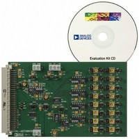
EVAL-AD7490CB Analog Devices Inc, EVAL-AD7490CB Datasheet - Page 5
EVAL-AD7490CB
Manufacturer Part Number
EVAL-AD7490CB
Description
BOARD EVAL FOR AD7490
Manufacturer
Analog Devices Inc
Datasheet
1.AD7490BRUZ.pdf
(28 pages)
Specifications of EVAL-AD7490CB
Number Of Adc's
1
Number Of Bits
12
Sampling Rate (per Second)
1M
Data Interface
Serial
Inputs Per Adc
16 Single Ended
Input Range
0 ~ 5 V
Power (typ) @ Conditions
12.5mW @ 1MSPS, 5 V
Voltage Supply Source
Single
Operating Temperature
-40°C ~ 85°C
Utilized Ic / Part
AD7490
Lead Free Status / RoHS Status
Contains lead / RoHS non-compliant


TIMING SPECIFICATIONS
V
Table 2. Timing Specifications
Parameter
f
t
t
t
t
t
t
t
t
t
t
t
t
t
t
1
2
3
4
5
SCLK
CONVERT
QUIET
2
3
3
4
5
6
7
8
9
10
11
12
Guaranteed by characterization. All input signals are specified with t
operating range spans from 2.7 V to 3.6 V. The 5 V operating range spans from 4.75 V to 5.25 V.
The mark/space ratio for the SCLK input is 40/60 to 60/40. The maximum SCLK frequency is 16 MHz with V
taken when interfacing to account for data access time, t
frequency with which the user’s system can operate (see the Serial Interface section).
Measured with the load circuit of Figure 2 and defined as the time required for the output to cross 0.4 V or 0.7 V
t
other device takes control of the bus between conversions, the user has to wait a maximum time of t
weakly driven to ADD3 between conversions, the user typically has to wait 17 ns at 3 V and 12 ns at 5 V after the CS falling edge before seeing ADD3 valid on DOUT.
t
back to remove the effects of charging or discharging the 25 pF capacitor. This means that the time, t
time of the part and is independent of the bus loading.
b
3
3
5
3
8
DD
b represents a worst-case figure for having ADD3 available on the DOUT line, that is, if the AD7490 goes back into three-state at the end of a conversion and some
is derived from the measured time taken by the data outputs to change 0.5 V when loaded with the circuit of Figure 2. The measured number is then extrapolated
4
2
= 2.7 V to 5.25 V, V
V
10
16
16 × t
50
12
20
30
60
0.4 × t
0.4 × t
15
15/50
20
5
20
1
DD
Limit at T
= 3 V
SCLK
SCLK
SCLK
DRIVE
MIN
V
10
20
16 × t
50
10
14
20
40
0.4 × t
0.4 × t
15
15/50
20
5
20
1
≤ V
DD
, T
= 5 V
1
MAX
DD
SCLK
SCLK
SCLK
, REF
IN
Unit
kHz min
MHz max
ns min
ns min
ns max
ns max
ns max
ns min
ns min
ns min
ns min/max
ns min
ns min
ns min
μs max
= 2.5 V; T
Figure 2. Load Circuit for Digital Output Timing Specifications
4
, and the setup time required for the user’s processor. These two times determine the maximum SCLK
TO OUTPUT
A
= T
R
MIN
PIN
= t
Description
Minimum quiet time required between bus relinquish and start of next conversion
CS to SCLK setup time
Delay from CS until DOUT three-state disabled
Delay from CS to DOUT valid
Data access time after SCLK falling edge
SCLK low pulse width
SCLK high pulse width
SCLK to DOUT valid hold time
SCLK falling edge to DOUT high impedance
DIN setup time prior to SCLK falling edge
DIN hold time after SCLK falling edge
16
Power-up time from full power-down/auto shutdown/auto standby modes
F
to T
Rev. C | Page 5 of 28
th
25pF
= 5 ns (10% to 90% of V
SCLK falling edge to CS high
C
L
MAX
200µA
200µA
, unless otherwise noted.
I
I
OL
OH
DD
) and timed from a voltage level of 1.6 V (see Figure 2). The 3 V
3
1.6V
8
b before having ADD3 valid on the DOUT line. If the DOUT line is
, quoted in the timing characteristics, is the true bus relinquish
DD
= 3 V to give a throughput of 870 kSPS. Care must be
DRIVE
.
AD7490
Related parts for EVAL-AD7490CB
Image
Part Number
Description
Manufacturer
Datasheet
Request
R

Part Number:
Description:
ENERCHIP CC EVAL KIT
Manufacturer:
Cymbet Corporation
Datasheet:

Part Number:
Description:
BOARD EVAL FOR AD976
Manufacturer:
Analog Devices Inc
Datasheet:

Part Number:
Description:
BOARD EVAL FOR ADXL345
Manufacturer:
Analog Devices Inc
Datasheet:

Part Number:
Description:
ENERCHIP CC SEH EVAL KIT
Manufacturer:
Cymbet Corporation
Datasheet:

Part Number:
Description:
ENERCHIP EP ENERGY HARVEST EVAL
Manufacturer:
Cymbet Corporation
Datasheet:

Part Number:
Description:
EVAL BOARD FOR TW6864-LB2-GR
Manufacturer:
Intersil
Datasheet:
Part Number:
Description:
EVAL BOARD FOR TW8816-LB3-GR
Manufacturer:
Intersil
Datasheet:
Part Number:
Description:
EVAL BOARD FOR TW8817-TA3-GRS
Manufacturer:
Intersil
Datasheet:

Part Number:
Description:
EVALUATION MODULE FOR ADUM4160
Manufacturer:
Analog Devices Inc
Datasheet:

Part Number:
Description:
BOARD EVALUATION ADCMP581BCP
Manufacturer:
Analog Devices Inc
Datasheet:
Part Number:
Description:
BOARD EVALUATION ADM1041
Manufacturer:
Analog Devices Inc
Datasheet:

Part Number:
Description:
EVAL BOARD FOR STM32F107VCT
Manufacturer:
STMicroelectronics
Datasheet:
Part Number:
Description:
BOARD EVAL FOR AD1954
Manufacturer:
Analog Devices Inc
Datasheet:
Part Number:
Description:
BOARD EVAL FOR AD1955
Manufacturer:
Analog Devices Inc
Datasheet:

Part Number:
Description:
BOARD EVAL FOR AD7655
Manufacturer:
Analog Devices Inc
Datasheet: