EVAL-AD7490CB Analog Devices Inc, EVAL-AD7490CB Datasheet - Page 6
EVAL-AD7490CB
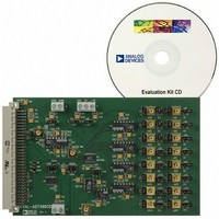
Manufacturer Part Number
EVAL-AD7490CB
Description
BOARD EVAL FOR AD7490
Manufacturer
Analog Devices Inc
Datasheet
1.AD7490BRUZ.pdf
(28 pages)
Specifications of EVAL-AD7490CB
Number Of Adc's
1
Number Of Bits
12
Sampling Rate (per Second)
1M
Data Interface
Serial
Inputs Per Adc
16 Single Ended
Input Range
0 ~ 5 V
Power (typ) @ Conditions
12.5mW @ 1MSPS, 5 V
Voltage Supply Source
Single
Operating Temperature
-40°C ~ 85°C
Utilized Ic / Part
AD7490
Lead Free Status / RoHS Status
Contains lead / RoHS non-compliant


AD7490
ABSOLUTE MAXIMUM RATINGS
T
Table 3.
Parameter
V
V
Analog Input Voltage to GND
Digital Input Voltage to GND
Digital Output Voltage to GND
REF
Input Current to Any Pin Except Supplies
Operating Temperature Ranges
Junction Temperature
LFCSP, TSSOP Package, Power Dissipation
Lead Temperature, Soldering
ESD
1
Transient currents of up to 100 mA do not cause SCR latch-up.
DD
DRIVE
A
Commercial (B Version)
Storage Temperature Range
θ
θ
Vapor Phase (60 sec)
Infrared (15 sec)
= 25°C, unless otherwise noted.
IN
to GND
JA
JC
to GND
to GND
Thermal Impedance
Thermal Impedance
1
Rating
−0.3 V to +7 V
−0.3 V to V
−0.3 V to V
−0.3 V to +7 V
−0.3 V to V
−0.3 V to V
±10 mA
−40°C to +85°C
−65°C to +150°C
150°C
97.9°C/W (TSSOP)
14°C/W (TSSOP)
215°C
220°C
1 kV
450 mW
108.2°C/W (LFCSP)
32.71°C/W (LFCSP)
DD
DD
DD
DD
+ 0.3 V
+ 0.3 V
+ 0.3 V
+ 0.3 V
Rev. C | Page 6 of 28
Stresses above those listed under Absolute Maximum Ratings
may cause permanent damage to the device. This is a stress
rating only; functional operation of the device at these or any
other conditions above those indicated in the operational
section of this specification is not implied. Exposure to absolute
maximum rating conditions for extended periods may affect
device reliability.
ESD CAUTION
Related parts for EVAL-AD7490CB
Image
Part Number
Description
Manufacturer
Datasheet
Request
R

Part Number:
Description:
ENERCHIP CC EVAL KIT
Manufacturer:
Cymbet Corporation
Datasheet:

Part Number:
Description:
BOARD EVAL FOR AD976
Manufacturer:
Analog Devices Inc
Datasheet:

Part Number:
Description:
BOARD EVAL FOR ADXL345
Manufacturer:
Analog Devices Inc
Datasheet:

Part Number:
Description:
ENERCHIP CC SEH EVAL KIT
Manufacturer:
Cymbet Corporation
Datasheet:

Part Number:
Description:
ENERCHIP EP ENERGY HARVEST EVAL
Manufacturer:
Cymbet Corporation
Datasheet:

Part Number:
Description:
EVAL BOARD FOR TW6864-LB2-GR
Manufacturer:
Intersil
Datasheet:
Part Number:
Description:
EVAL BOARD FOR TW8816-LB3-GR
Manufacturer:
Intersil
Datasheet:
Part Number:
Description:
EVAL BOARD FOR TW8817-TA3-GRS
Manufacturer:
Intersil
Datasheet:

Part Number:
Description:
EVALUATION MODULE FOR ADUM4160
Manufacturer:
Analog Devices Inc
Datasheet:

Part Number:
Description:
BOARD EVALUATION ADCMP581BCP
Manufacturer:
Analog Devices Inc
Datasheet:
Part Number:
Description:
BOARD EVALUATION ADM1041
Manufacturer:
Analog Devices Inc
Datasheet:

Part Number:
Description:
EVAL BOARD FOR STM32F107VCT
Manufacturer:
STMicroelectronics
Datasheet:
Part Number:
Description:
BOARD EVAL FOR AD1954
Manufacturer:
Analog Devices Inc
Datasheet:
Part Number:
Description:
BOARD EVAL FOR AD1955
Manufacturer:
Analog Devices Inc
Datasheet:

Part Number:
Description:
BOARD EVAL FOR AD7655
Manufacturer:
Analog Devices Inc
Datasheet: