EVAL-AD9831EB Analog Devices Inc, EVAL-AD9831EB Datasheet
EVAL-AD9831EB
Specifications of EVAL-AD9831EB


Related parts for EVAL-AD9831EB


EVAL-AD9831EB Summary of contents
Page 1
FEATURES 3 V/5 V Power Supply 25 MHz Speed On-Chip SINE Look-Up Table On-Chip 10-Bit DAC Parallel Loading Powerdown Option 72 dB SFDR 125 Power Consumption Power Consumption 48-Pin TQFP APPLICATIONS DDS ...
Page 2
AD9831–SPECIFICATIONS Parameter SIGNAL DAC SPECIFICATIONS Resolution Update Rate (f ) MAX I Full Scale OUT Output Compliance DC Accuracy Integral Nonlinearity Differential Nonlinearity 2 DDS SPECIFICATIONS Dynamic Specifications Signal to Noise Ratio Total Harmonic Distortion Spurious Free Dynamic Range (SFDR) ...
Page 3
TIMING CHARACTERISTICS Limit MIN MAX Parameter (A Version ...
Page 4
... Exposure to absolute maximum rating conditions for extended periods may affect device reliability. ORDERING GUIDE Temperature Model Range AD9831AST – +85 C 48-Pin TQFP ST-48 EVAL-AD9831EB Evaluation Board *ST = Thin Quad Flatpack (TQFP). AGND REFOUT SLEEP DVDD DVDD DGND ...
Page 5
Mnemonic Function POWER SUPPLY AVDD Positive power supply for the analog section. A 0.1 F decoupling capacitor should be connected between AVDD and AGND. AVDD can have a value AGND Analog Ground. DVDD Positive power supply for ...
Page 6
AD9831 TERMINOLOGY Integral Nonlinearity This is the maximum deviation of any code from a straight line passing through the endpoints of the transfer function. The endpoints of the transfer function are zero scale, a point 0.5 LSB below the first ...
Page 7
+3. MCLK FREQUENCY – MHz Figure 5. Typical Current Consumption vs. MCLK Frequency – 1/3 OUT MCLK AVDD = DVDD = +3.3V –55 ...
Page 8
AD9831–Typical Performance Characteristics 10 AVDD = DVDD = +2.97V 7.5 5.0 2.5 0 –40 –30 –20 TEMPERATURE – C Figure 11. Wake-Up Time vs. Temperature 0 –10 –20 –30 –40 –50 –60 –70 –80 –90 –100 START 0Hz RBW 300Hz ...
Page 9
START 0Hz RBW 300Hz VBW 1kHz Figure 17 MHz 6.1 MHz, Frequency MCLK OUT Word = 3E76C8B4 0 –10 –20 –30 –40 –50 –60 ...
Page 10
AD9831 CIRCUIT DESCRIPTION The AD9831 provides an exciting new level of integration for the RF/Communications system designer. The AD9831 com- bines the Numerical Controlled Oscillator (NCO), SINE Look- Up Table, Frequency and Phase Modulators, and a Digital-to- Analog Converter on ...
Page 11
DSP and MPU Interfacing The AD9831 has a parallel interface, with 16 bits of data being loaded during each write cycle. The frequency or phase registers are loaded by asserting the WR signal. The destination register for the 16 bit ...
Page 12
AD9831 APPLICATIONS The AD9831 contains functions which make it suitable for modulation applications. The part can be used to perform simple modulation such as FSK. More complex modulation schemes such as GMSK and QPSK can also be implemented using the ...
Page 13
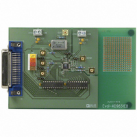
... Prototyping Area An area is available on the evaluation board where the user can add additional circuits to the evaluation test set. Users may want to build custom analog filters for the output or add buffers and operational amplifiers which are to be used in the final application ...
Page 14
... PSEL0 10 LK3 FSELECT MCLK 7 MCLK DVDD 3 SLEEP LK4 DVDD DGND DVDD U1 OUT XTAL1 DGND Figure 24. AD9831 Evaluation Board Layout Links LK1–LK4 LK5 Switch SW Sockets MCLK, PSEL0, PSEL1, FSELECT, IOUT, REFIN Connectors J1 J2, J3 –14– AVDD C4, C5, C6 0.1µF DVDD AVDD ...
Page 15
REV. A OUTLINE DIMENSIONS Dimensions shown in inches and (mm). Thin Quad Flatpack (TQFP) ST-48 0.063 (1.60) MAX 0.354 (9.00) BSC 0.030 (0.75) 0.057 (1.45) 0.276 (7.0) BSC 0.030 (0.75) 0.018 (0.45) 0.053 (1.35) 0.018 (0.45 SEATING PLANE ...
Page 16
–16– ...