AD9956/PCB Analog Devices Inc, AD9956/PCB Datasheet - Page 23
AD9956/PCB
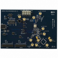
Manufacturer Part Number
AD9956/PCB
Description
BOARD EVAL FOR AD9956
Manufacturer
Analog Devices Inc
Datasheet
1.AD9956YCPZ.pdf
(32 pages)
Specifications of AD9956/PCB
Module/board Type
Evaluation Board
For Use With/related Products
AD9956
Lead Free Status / RoHS Status
Contains lead / RoHS non-compliant


INSTRUCTION BYTE
The instruction byte contains the following information:
Table 4.
D7
R/Wb
R/Wb—Bit 7 of the instruction byte determines whether a read
or write data transfer occurs after the instruction byte write.
Logic 1 indicates a read operation. Logic 0 indicates a write
operation.
X, X—Bits 6 and 5 of the instruction byte are Don’t Care.
A4 to A0—Bits 4 to 0 of the instruction byte determine which
register is accessed during the data transfer portion of the
communications cycle.
SERIAL INTERFACE PORT PIN DESCRIPTION
SCLK—Serial Clock. The serial clock pin is used to synchronize
data to and from the AD9956 and to run the internal state
machines. The SCLK maximum frequency is 25 MHz.
CS —Chip Select Bar. CS is an active low input that allows more
than one device on the same serial communications line. The
SDO and SDI/O pins go to a high impedance state when this
input is high. If driven high during any communications cycle,
that cycle is suspended until CS is reactivated low. Chip select
can be tied low in systems that maintain control of SCLK.
SDI/O—Serial Data Input/Output. Data is always written to the
AD9956 on this pin. However, this pin can be used as a bidirec-
tional data line. CFR1<7> controls the configuration of this pin.
The default value (0) configures the SDI/O pin as bidirectional.
SDO—Serial Data Out. Data is read from this pin for protocols
that use separate lines for transmitting and receiving data. When
the AD9956 operates in a single bidirectional I/O mode, this pin
does not output data and is set to a high impedance state.
I/O_RESET—A high signal on this pin resets the I/O port state
machines without affecting the addressable registers’ contents.
An active high input on the I/O_RESET pin causes the current
communication cycle to abort. After I/O_RESET returns low
(0), another communication cycle can begin, starting with the
instruction byte write. Note that when not in use, this pin
should be forced low, because it floats to the threshold value.
D6
X
D5
X
D4
A4
D3
A3
D2
A2
D1
A1
D0
A0
Rev. A | Page 23 of 32
MSB/LSB TRANSFERS
The AD9956 serial port can support both most significant bit
(MSB) first or least significant bit (LSB) first data formats. This
functionality is controlled by the LSB first bit in Control
Register 1 (CFR1<15>). The default value of this bit is low
(MSB first). When CFR1 <15> is set high, the AD9956 serial
port is in LSB first format. The instruction byte must be written
in the format indicated by CFR1 <15>. If the AD9956 is in LSB
first mode, the instruction byte must be written from least
significant bit to most significant bit. However, the instruction
byte phase of the communications cycle still precedes the data
transfer cycle.
For MSB first operation, all data written to (read from) the
AD9956 are in MSB first order. If the LSB mode is active, all
data written to (read from) the AD9956 are in LSB first order.
SCLK
SDI/O
SCLK
SDI/O
SDO
CS
CS
SYMBOL
T
T
DV
SCLKR
SYMBOL
T
T
T
T
PRE
SCLKW
DSU
DHLD
Figure 33. Timing Diagram for Data Write to AD9956
Figure 34. Timing Diagram for Data Read to AD9956
T
T
PRE
DSU
MAX
40ns
400ns
FIRST BIT
FIRST BIT
MIN
6ns
40ns
6.5ns
0ns
T
DEFINITION
DATA VALID TIME
PERIOD OF SERIAL DATA CLOCK (READ)
DHLD
T
T
SCLKR
SCLKW
DEFINITION
CS SETUP TIME
PERIOD OF SERIAL DATA CLOCK (WRITE)
SERIAL DATA SETUP TIME
SERIAL DATA HOLD TIME
T
DV
SECOND BIT
SECOND BIT
AD9956
Related parts for AD9956/PCB
Image
Part Number
Description
Manufacturer
Datasheet
Request
R

Part Number:
Description:
400 Msps 14 Bit DDS EvBd. W/2450MHz VCO
Manufacturer:
Analog Devices Inc
Datasheet:
Part Number:
Description:
400 Msps 14 Bit DDS Eval Bd.
Manufacturer:
Analog Devices Inc
Datasheet:
Part Number:
Description:
BOARD EVAL 14BIT 1.8V 48LFCSP
Manufacturer:
Analog Devices Inc
Datasheet:


Part Number:
Description:
±1.7g Dual-Axis IMEMS Accelerometer Evaluation Board
Manufacturer:
Analog Devices Inc
Datasheet:
Part Number:
Description:
Inertial Sensor Evaluation System
Manufacturer:
Analog Devices Inc
Datasheet:
Part Number:
Description:
Manufacturer:
Analog Devices Inc
Datasheet:
Part Number:
Description:
Manufacturer:
Analog Devices Inc
Datasheet:
Part Number:
Description:
Manufacturer:
Analog Devices Inc
Datasheet:
Part Number:
Description:
Manufacturer:
Analog Devices Inc
Datasheet:
Part Number:
Description:
Manufacturer:
Analog Devices Inc
Datasheet:
Part Number:
Description:
Manufacturer:
Analog Devices Inc
Datasheet:
Part Number:
Description:
Manufacturer:
Analog Devices Inc
Datasheet: